

Philips 74lv423 DATASHEETS
INTEGRATED CIRCUITS
74LV423
Dual retriggerable monostable
multivibrator with reset
Product specification 1997 Feb 04
IC24 Data Handbook
Philips Semiconductors Preliminary specification
Dual retriggerable monostable multivibrator
with reset
FEA TURES
•Optimized for Low Voltage applications: 1.0 to 5.5V
•Accepts TTL input levels between V
•Typical V
T
amb
•Typical V
T
amb
(output ground bounce) 0.8V @ VCC = 3.3V,
OLP
= 25°C
(output VOH undershoot) 2V @ VCC = 3.3V,
OHV
= 25°C
= 2.7V and VCC = 3.6V
CC
•DC triggered from active HIGH or active LOW inputs
•Retriggerable for very long pulses up to 100% duty factor
•Direct reset terminates output pulses
•Schmitt-trigger action on all inputs except for the reset input
•Output capability: standard (except for nR
•I
category: MSI
CC
EXT/CEXT
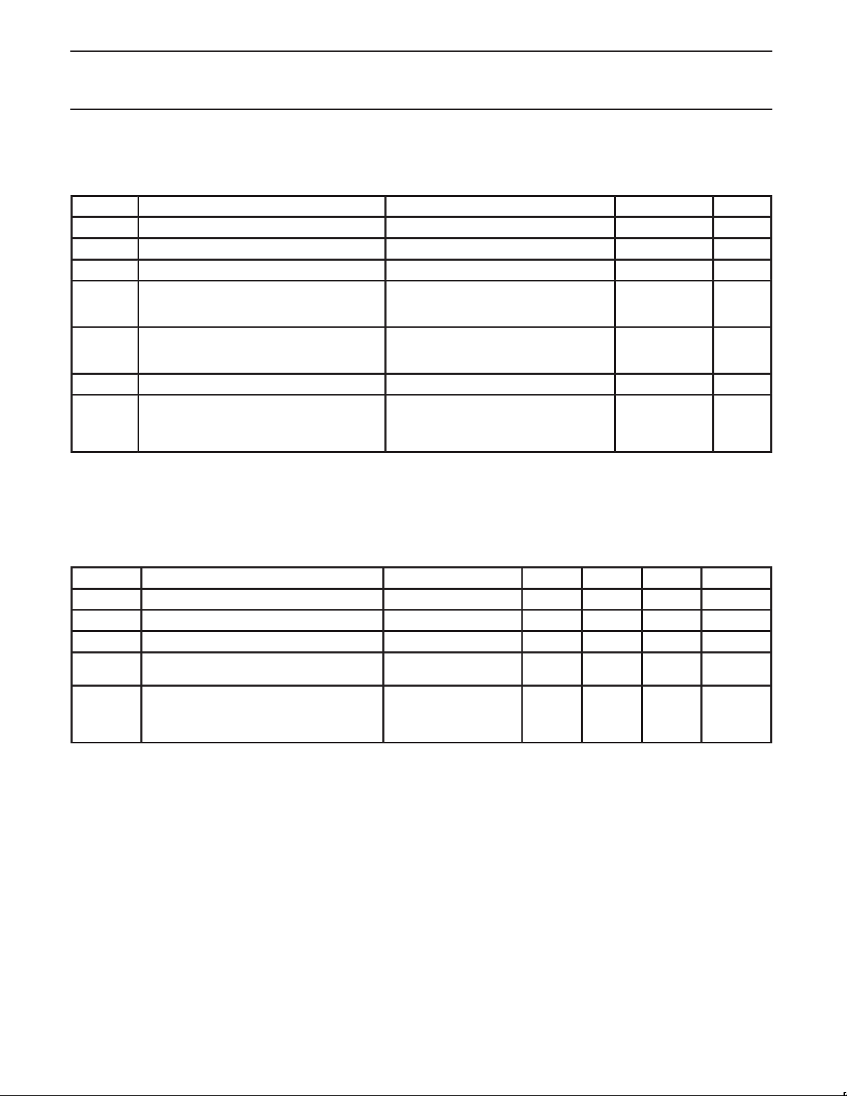
QUICK REFERENCE DATA
GND = 0V; T
SYMBOL
t
PHL/tPLH
C
I
C
PD
NOTES:
is used to determine the dynamic power dissipation (PD in µW)
1. C
PD
= CPD V
P
D
= input frequency in MHz; CL = output load capacity in pF;
f
i
= output frequency in MHz; VCC = supply voltage in V;
f
o
(C
= 25°C; tr = tf 2.5 ns
amb
CC
2
V
L
fo) = sum of the outputs.
CC
PARAMETER CONDITIONS TYPICAL UNIT
Propagation delay
, nB to nQ, nQ
nA
nRD to nQ, nQ
Input capacitance 3.5 pF
Power dissipation capacitance per flip-flop VCC = 3.3V, VI = GND to V
2
fi (CL V
2
fo) where:
CC
)
DESCRIPTION
The 74LV423 is a low-voltage Si-gate CMOS device and is pin and
function compatible with the 74HC/HCT423.
The 74LV423 is a dual retriggerable monostable multivibrator with
output pulse width control by three methods. The basic pulse time is
programmed by selection of an external resistor (R
capacitor (C
Figure 1. Once triggered, the basic output pulse width may be
extended by retriggering the gated active LOW-going edge input
(nA
process, the output pulse period (nQ = HIGH, nQ
made as long as desired. Alternatively, an output delay can be
terminated at any time by a LOW-going edge on input nR
also inhibits the triggering. Figures 2 and 3 illustrate pulse control by
retriggering and early reset. The basic output pulse width is
essentially determined by the values of the external timing
components R
see Figure 6. When C
width is defined as: t
t
W
C
EXT
nB inputs makes the circuit highly tolerant of slower input rise and
fall times.
CL = 15pF
= 3.3V
V
CC
= 5KΩ
R
EXT
= 0pF
C
EXT
74L V423
) and
). They are normally connected as shown in
EXT
) or the active HIGH-going edge input (nB). By repeating this
and C
EXT
= pulse width in ns; R
= external capacitor in pF. Schmitt-trigger action in the nA and
CC
. For pulse width when C
EXT
10,000pF, the typical output pulse
EXT
= 0.45 R
W
= external resistor in KΩ; and
EXT
1
C
EXT
16
13
17 pF
EXT
= LOW) can be
EXT
(typ.), where
EXT
, which
D
<10000pF,
ns
ns
ORDERING INFORMATION
PACKAGES TEMPERATURE RANGE OUTSIDE NORTH AMERICA NORTH AMERICA PKG. DWG. #
16-Pin Plastic DIL –40°C to +125°C 74LV423 N 74LV423 N SOT38-1
16-Pin Plastic SO –40°C to +125°C 74LV423 D 74LV423 D SOT109-1
16-Pin Plastic SSOP Type II –40°C to +125°C 74LV423 DB 74LV423 DB SOT338-1
16-Pin Plastic TSSOP Type I –40°C to +125°C 74L V423 PW 74LV423PW DH SOT403-1
1997 Feb 04 853–1913 17724
2
Philips Semiconductors Preliminary specification
Dual retriggerable monostable multivibrator
with reset
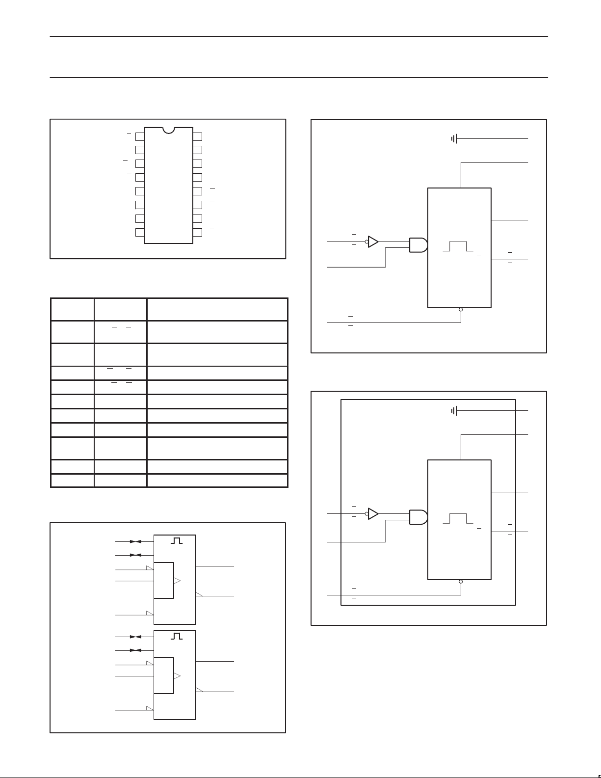
PIN CONFIGURATION
1A
1
1B
2
1R
3
D
1Q
4
5
2Q
6
2C
EXT
GND
7
8
2R
EXT/CEXT
PIN DESCRIPTION
PIN
NUMBER
1,9 1A, 2A
2,10 1B, 2B
3,11 1RD, 2RDDirect reset LOW
4, 12 1Q, 2Q Outputs (active LOW)
7 2R
8 GND Ground (0V)
13, 5 1Q, 2Q Outputs (active HIGH)
14, 6
15 1R
16 V
SYMBOL FUNCTION
Trigger inputs
(negative-edge triggered)
Trigger inputs
(positive-edge triggered)
EXT/CEXT
1C
EXT,
2C
EXT
EXT/CEXT
CC
External resistor/capacitor connection
External capacitor connection
External resistor/capacitor connection
Positive supply voltage
LOGIC SYMBOL (IEEE/IEC)
14
15
1
2
3
6
7
9
10
CX
RCX
&
R
CX
RCX
&
V
16
CC
15
1R
EXT/CEXT
14
1C
EXT
13
1Q
12
2Q
11
2R
D
10
2B
9
2A
SV00096
13
4
5
12
LOGIC SYMBOL
1
1A
2A
9
2
1B
10
2B
3
1R
D
11
2R
D
FUNCTIONAL DIAGRAM
1
1A
2A
9
1B
2
2B
10
1R
3
D
2R
11
D
74L V423
14
1C
EXT
6
2C
EXT
1R
EXT/CEXT
2R
EXT/CEXT
S
Q
T
Q
R
D
1R
EXT/CEXT
2R
EXT/CEXT
S
Q
T
Q
R
D
15
7
1Q
13
2Q
5
1Q
4
2Q
12
SV00160
14
1C
EXT
2C
6
EXT
15
7
1Q
13
2Q
5
1Q
4
2Q
12
SV00162
1997 Feb 04
11
R
SV00161
3
Philips Semiconductors Preliminary specification
Dual retriggerable monostable multivibrator
with reset
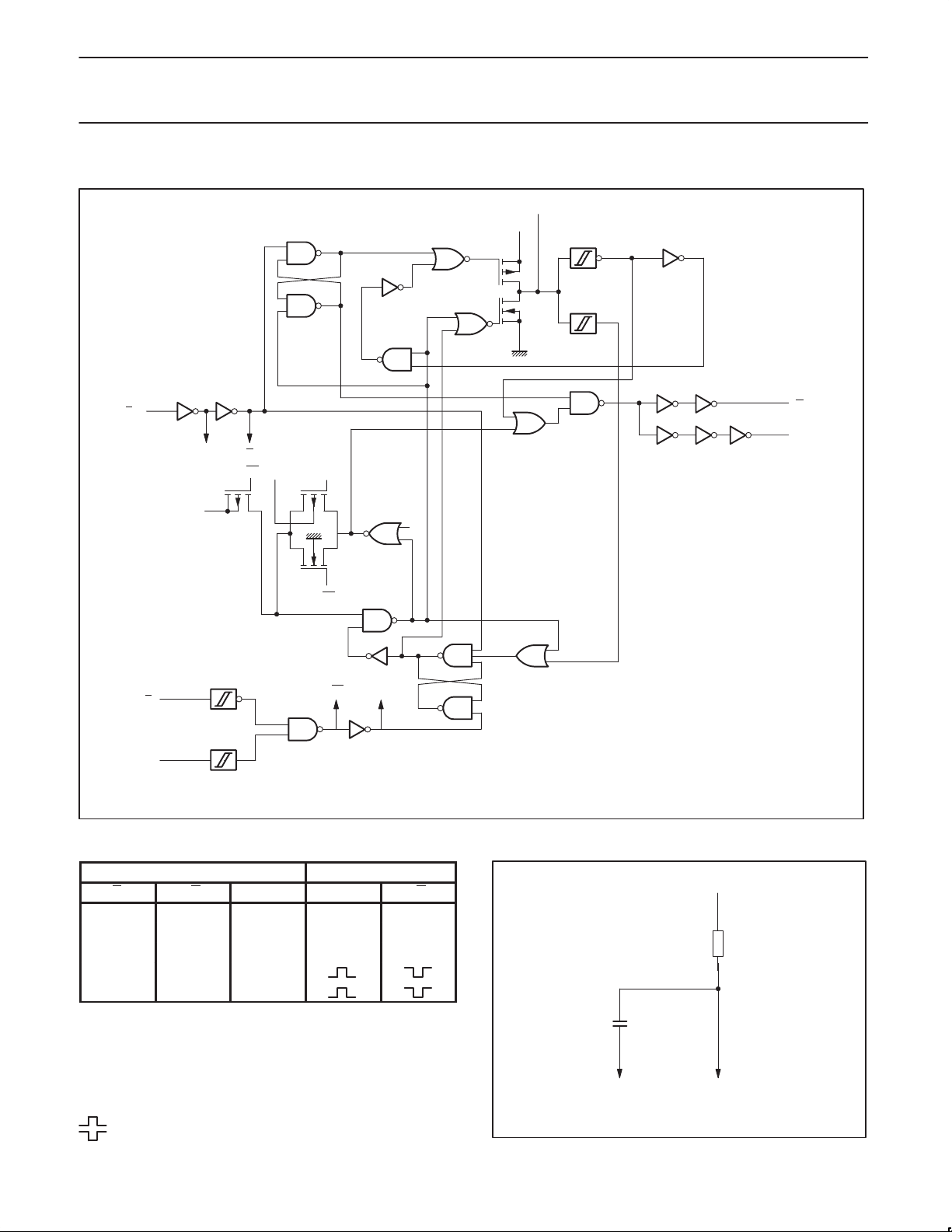
LOGIC DIAGRAM
R
D
RR
CLCLV
CC
V
CC
CL
R
nR
V
CC
74L V423
EXT/CEXT
Q
Q
A
B
It is recommended that Pin 6 (2C
CLCL
) and Pin 14 (1C
EXT
FUNCTION TABLE
INPUTS OUTPUTS
nR
D
L X X L H
X H X L * H *
X X L L * H *
H L ↑
H ↓ H
NOTES:
* If the monostable was triggered before this condition was
established, the pulse will continue as programmed.
H = HIGH voltage level
L = LOW voltage level
X = don’t care
↑ = LOW-to-HIGH transition
↓ = HIGH-to-LOW transition
= one HIGH level output pulse
= one LOW level output pulse
nA nB nQ nQ
) by externally grounded to Pin 8 (GND)
EXT
C
EXT
to nC
EXT
(pin 14 or 6)
Figure 1. Timing Component Connection
V
CC
to nR
EXT/CEXT
(pin 15 or 7)
SV00163
R
EXT
SV00101
1997 Feb 04
4
Philips Semiconductors Preliminary specification
Dual retriggerable monostable multivibrator
74L V423
with reset
ABSOLUTE MAXIMUM RATINGS
In accordance with the Absolute Maximum Rating System (IEC 134).
Voltages are referenced to GND (ground = 0V).
SYMBOL
I
I
V
CC
DC supply voltage –0.5 to +7.0 V
DC input diode current VI < –0.5 or VI > VCC + 0.5V 20 mA
IK
DC output diode current VO < –0.5 or VO > VCC + 0.5V 50 mA
OK
DC output source or sink current
I
– standard outputs
O
– bus driver outputs
DC VCC or GND current for types with
I
,
I
T
GND
stg
– standard outputs
– bus driver outputs
CC
Storage temperature range –65 to +150 °C
Power dissipation per package
P
TOT
– plastic DIL
– plastic mini-pack (SO)
– plastic shrink mini-pack (SSOP and TSSOP)
NOTES:
1. Stresses beyond those listed may cause permanent damage to the device. These are stress ratings only and functional operation of the
device at these or any other conditions beyond those indicated under “recommended operating conditions” is not implied. Exposure to
absolute-maximum-rated conditions for extended periods may affect device reliability .
2. The input and output voltage ratings may be exceeded if the input and output current ratings are observed.
PARAMETER CONDITIONS RATING UNIT
1, 2
–0.5V < VO < VCC + 0.5V
for temperature range: –40 to +125°C
above +70°C derate linearly with 12 mW/K
above +70°C derate linearly with 8 mW/K
above +60°C derate linearly with 5.5 mW/K
25
35
50
70
750
500
500
mA
mA
mW
RECOMMENDED OPERATING CONDITIONS
SYMBOL PARAMETER CONDITIONS MIN TYP MAX UNIT
V
CC
V
V
T
amb
tr, t
NOTE:
1. The LV is guaranteed to function down to V
DC supply voltage See Note 1 1.2 3.3 5.5 V
Input voltage 0 – V
I
Output voltage 0 – V
O
Operating ambient temperature range in free
air
Input rise and fall times except for
f
Schmitt-trigger inputs
= 1.0V (input levels GND or VCC); DC characteristics are guaranteed from VCC = 1.2V to VCC = 5.5V.
CC
See DC and AC
characteristics per device
VCC = 1.0V to 2.0V
= 2.0V to 2.7V
V
CC
= 2.7V to 3.6V
V
CC
= 3.6V to 5.5V
V
CC
–40
–40
–
–
–
–
–
–
–
CC
CC
+85
+125
500
200
100
50
V
V
°C
ns/V
1997 Feb 04
5
 Loading...