

Philips 74LV4094PW, 74LV4094N, 74LV4094DB, 74LV4094D Datasheet
74LV4094
8-stage shift-and-store bus register
Product specification 1998 Jun 23
INTEGRATED CIRCUITS
Philips Semiconductors Product specification
74L V40948-stage shift-and-store bus register
2
1998 Jun 23 853-2078 19619
FEA TURES
•Optimized for low voltage applications: 1.0 to 3.6 V
•Accepts TTL input levels between V
CC
= 2.7 V and V
CC
= 3.6 V
•Typical V
OLP
(output ground bounce) < 0.8 V at V
CC
= 3.3 V ,
T
amb
= 25°C
•Typical V
OHV
(output VOH undershoot) > 2 V at V
CC
= 3.3 V ,
T
amb
= 25°C
•Output capability: standard
•I
CC
category: MSI
Applications:
•Serial-to-parallel data conversion
•Remote control holding register
DESCRIPTION
The 74LV4094 is a low-voltage Si-gate CMOS device and is pin and
function compatible with 74HC/HCT4094.
The 74LV4094 is an 8-stage serial shift register having a storage
latch associated with each stage for strobing data from the serial
input (D) to the parallel buffered 3-State outputs (QP
0
to OP7). The
parallel outputs may be connected directly to the common bus lines.
Data is shifted on the positive-going clock (CP) transitions. The data
in each shift register is transferred to the storage register when the
strobe input (STR) is HIGH. Data in the storage register appears at
the outputs whenever the output enable input (OE) signal is HIGH.
Two serial outputs (QS
1
and QS2) are available for cascading a
number of 74LV4094 devices. Data is available at QS
1
on the
positive-going clock edges to allow high-speed operation in
cascaded systems in which the clock rise time is fast. The same
serial information is available at QS
2
on the next negative going
clock edge and is for cascading 74LV4094 devices when the clock
rise time is slow.
QUICK REFERENCE DA TA
GND = 0 V; T
amb
= 25°C; tr =t
f
≤ 2.5 ns
SYMBOL
PARAMETER CONDITIONS TYPICAL UNIT
t
PHL/tPLH
Propagation delay
CP to QS
1
CP to QS
2
CP to QP
n
STR to QP
n
CL = 15 pF;
VCC = 3.3 V
14
13
18
17
ns
f
MAX
Maximum clock frequency
95
MHz
C
I
Input capacitance 3.5 pF
C
PD
Power dissipation capacitance per gate
VCC = 3.3 V
VI = GND to V
CC
NO TAG
83 pF
NOTE:
1. C
PD
is used to determine the dynamic power dissipation (PD in µW)
P
D
= CPD × V
CC
2
× fi (CL × V
CC
2
× fo) where:
f
i
= input frequency in MHz; CL = output load capacity in pF;
f
o
= output frequency in MHz; VCC = supply voltage in V;
(C
L
× V
CC
2
× fo) = sum of the outputs.
ORDERING INFORMATION
PACKAGES TEMPERATURE RANGE OUTSIDE NORTH AMERICA NORTH AMERICA PKG. DWG. #
16-Pin Plastic DIL –40°C to +125°C 74LV4094 N 74LV4094 N SOT38-4
16-Pin Plastic SO –40°C to +125°C 74LV4094 D 74LV4094 D SOT109-1
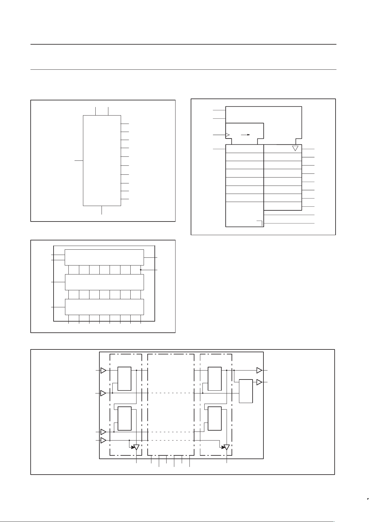
PIN CONFIGURATION
SV01611
1
2
3
4
5
6
STR
D
CP
QP
0
QP
1
QP
2
V
CC
OE
QP
4
16
15
14
13
12
11
7
8
GND
QS
2
QS
1
10
9
QP
3
QP
5
QP
6
QP
7
PIN DESCRIPTION
PIN NUMBER SYMBOL FUNCTION
1 STR Strobe input
2 D Serial input
3 CP Clock input
4, 5, 6, 7, 14,
13, 12, 11
QP0 to QP7Parallel outputs
8 GND Ground (0 V)
9, 10 QS1, QS
2
Serial outputs
15 OE Output enable input
16 V
CC
Positive supply voltage
Philips Semiconductors Product specification
74LV40948-stage shift-and-store bus register
1998 Jun 23
3
LOGIC SYMBOL
SV01612
1
2
3
4
5
6
STR
D
CP
QP
0
QP
1
QP
2
OE
QP
4
QP
5
QP
6
QP
7
15
14
13
12
11
7
QP
3
QS
2
QS
1
10
9
FUNCTIONAL DIAGRAM
3-STATE OUTPUTS
8-STATE SHIFT
REGISTER
8-BIT STORAGE
REGISTER
SV01614
2
3
1
15
D
CP
STR
OE
QS
2
QS
1
QP0QP1QP2QP3QP4Q51QP6QP
7
9
10
4 5 6 7 14 13 12 11
LOGIC SYMBOL (IEEE/IEC)
SV01613
4
5
6
7
14
13
12
11
9
10
2D
3
1D
C2
EN3
1
15
3
2
SRG8
C1/
LOGIC DIAGRAM
SV01615
DCPQ
latch
D
CP
D
CP
D
CP
D
CP
D
CP
Q
Q
Q
Q
Q
FF0 FF7
latch latch
STAGE 0 STAGE 7
STAGES 1 TO 6
D
CP
STR
OE
QP0QP
1
QP
2
QP
3
QP
4
QP
5
QP
6
QP
7
Q
7
’
QS
2
Philips Semiconductors Product specification
74LV40948-stage shift-and-store bus register
1998 Jun 23
4
FUNCTION TABLE
INPUTS PARALLEL OUTPUT SERIAL OUTPUTS
CP OE STR D QP
0
QP
n
QS
1
QS
2
↑ L X X Z Z Q’
6
NC
↓ L X X Z Z NC QP
7
↑ H L X NC NC Q’
6
NC
↑ H H L L QP
n–1
Q’
6
NC
↑ H H H H QP
n–1
Q’
6
NC
↓ H H H NC NC NC QP
7
NOTES:
H = HIGH voltage level
L = LOW voltage level
X = don’t care
Z = high impedance OFF-state
NC = no change
↑ = LOW-to–HIGH CP transition
↓ = HIGH-to-LOW CP transition
Q’
6
= the information in the 8th register stage is transferred to the
8
th
register stage and QSn clock edge.
TIMING DIAGRAM
SV01616
CPCLOCK INPUT
DATA INPUT
STROBE INPUT
OUTPUT ENABLE INPUT
INTERNAL Q’0 (FF0)
OUTPUT
INTERNAL Q’6 (FF6)
OUTPUT
Z–state
Z–state
SERIAL OUTPUT
SERIAL OUTPUT
D
STR
OE
QP
0
QP
6
QS
2
QS
1
Philips Semiconductors Product specification
74LV40948-stage shift-and-store bus register
1998 Jun 23
5
ABSOLUTE MAXIMUM RATINGS
NO TAG, NO TAG
In accordance with the Absolute Maximum Rating System (IEC 134).
Voltages are referenced to GND (ground = 0 V).
SYMBOL
PARAMETER CONDITIONS RATING UNIT
V
CC
DC supply voltage –0.5 to +7.0 V
I
IK
DC input diode current VI < –0.5 or VI > VCC + 0.5V 20 mA
I
OK
DC output diode current VO < –0.5 or VO > VCC + 0.5V 50 mA
I
O
DC output source or sink current
– standard outputs
–0.5V < VO < VCC + 0.5V
25
mA
I
GND
,
I
CC
DC VCC or GND current for types with
– standard outputs 50
mA
T
stg
Storage temperature range –65 to +150 °C
P
TOT
Power dissipation per package
– plastic DIL
– plastic mini-pack (SO)
– plastic shrink mini-pack (SSOP and TSSOP)
for temperature range: –40 to +125°C
above +70°C derate linearly with 12 mW/K
above +70°C derate linearly with 8 mW/K
above +60°C derate linearly with 5.5 mW/K
750
500
400
mW
NOTES:
1. Stresses beyond those listed may cause permanent damage to the device. These are stress ratings only and functional operation of the
device at these or any other conditions beyond those indicated under “recommended operating conditions” is not implied. Exposure to
absolute-maximum-rated conditions for extended periods may affect device reliability .
2. The input and output voltage ratings may be exceeded if the input and output current ratings are observed.
RECOMMENDED OPERATING CONDITIONS
SYMBOL PARAMETER CONDITIONS MIN TYP MAX UNIT
V
CC
DC supply voltage See Note NO TAG 1.0 3.3 3.6 V
V
I
Input voltage 0 – V
CC
V
V
O
Output voltage 0 – V
CC
V
T
amb
Operating ambient temperature range in free air
See DC and AC
characteristics
–40
–40
+85
+125
°C
tr, t
f
Input rise and fall times except for
Schmitt-trigger inputs
VCC = 1.0V to 2.0V
VCC = 2.0V to 2.7V
VCC = 2.7V to 3.6V
–
–
–
–
–
–
500
200
100
ns/V
NOTE:
1. The LV is guaranteed to function down to V
CC
= 1.0V (input levels GND or VCC); DC characteristics are guaranteed from VCC = 1.2V to VCC = 5.5V.
 Loading...