

Philips 74LV4066U, 74LV4066PW, 74LV4066N, 74LV4066DB, 74LV4066D Datasheet
74LV4066
Quad bilateral switches
Product specification
Supersedes data of 1996 Jan 01
IC24 Data Handbook
1998 Jun 23
INTEGRATED CIRCUITS
Philips Semiconductors Product specification
74L V4066Quad bilateral switches
2
1998 Jun 23 853-2077 19619
FEA TURES
•Optimized for Low Voltage applications: 1.0V to 6.0V
•Accepts TTL input levels between V
CC
= 2.7 V and V
CC
= 3.6 V
•Typical V
OLP
(output ground bounce) < 0.8 V at VCC = 3.3 V,
T
amb
= 25 °C.
• Very low typ “ON” resistance:
25 at V
CC
– VEE = 4.5 V
35 at VCC – VEE = 3.0 V
60 at V
CC
– VEE = 2.0 V
•Output capability: non-standard
•I
CC
category: SSI
DESCRIPTION
The 74LV4066 is a low-voltage Si-gate CMOS device that is pin and
function compatible with 74HC/HCT4066.
The 74LV4066 has four independent analog switches. Each switch
has two input/output terminals (nY, nZ) and an active HIGH enable
input (nE). When nE is LOW the corresponding analog switch is
turned off.
The 74LV4066 has an on resistance which is dramatically reduced
in comparison with 74HCT4066.
FUNCTION TABLE
INPUTS
nE
SWITCH
L off
H on
NOTES:
H = HIGH voltage level
L = LOW voltage level
QUICK REFERENCE DA TA
GND = 0 V; T
amb
= 25°C; tr =tf 2.5 ns
SYMBOL PARAMETER CONDITIONS TYPICAL UNIT
t
PZH/tPZL
Turn “ON” time: nE to V
OS
CL = 15pF
10 ns
t
PHZ/tPLZ
Turn “OFF” time: nE to V
OS
R
L
=
1K
VCC= 3.3V
13 ns
C
I
Input capacitance 3.5 pF
C
PD
Power dissipation capacitance per switch Notes 1, 2 11 pF
C
S
Maximum switch capacitances 8 pF
NOTES:
1. C
PD
is used to determine the dynamic power dissipation (PD in µW)
P
D
= CPD × V
CC
2
× fi (CL × V
CC
2
× fo) where:
f
i
= input frequency in MHz; CL = output load capacity in pF;
f
o
= output frequency in MHz; Cs = maximum switch capacitance in pF;
{(C
L
+ CS) × V
CC
2
× Fo} = sum of the outputs.
V
CC
= supply voltage in V .
2. The condition is V
I
= GND to V
CC.
ORDERING AND PACKAGE INFORMA TION
PACKAGES
TYPE NUMBER
PINS PACKAGE MATERIAL CODE
74LV4066N 16 DIL Plastic SOT27-1
74LV4066D 16 SO Plastic SOT108-1
74LV4066DB 16 SSOP Plastic SOT337-1
74LV4066PW 16 TSSOP Plastic SOT402-1
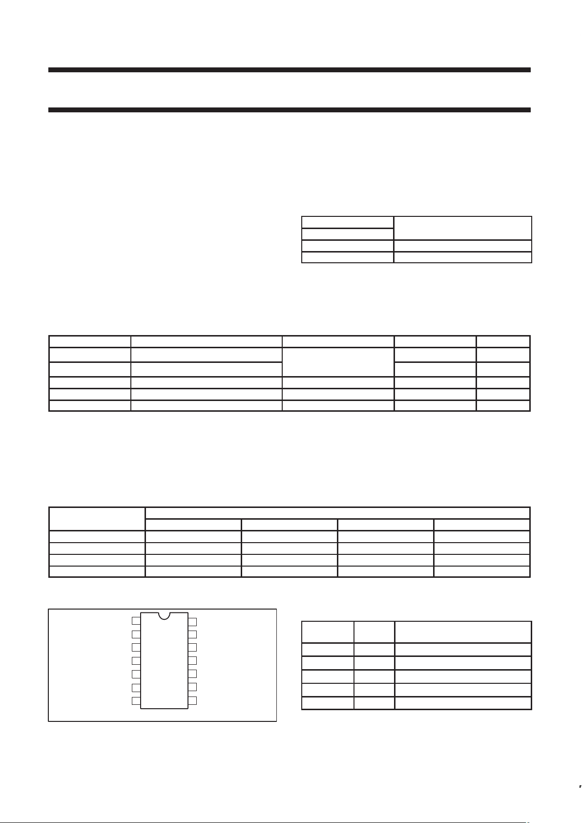
PIN CONFIGURATION
SV01669
12
11
10
9
8
7
6
5
4
3
2
1
13
14
GND
V
CC
1Y
1Z
2Z
2Y
2E
3E
1E
4E
4Y
4Z
3Z
3Y
PIN DESCRIPTION
PIN
NUMBER
SYMBOL FUNCTION
1, 4, 8, 11 1Y – 4Y Independent inputs/outputs
2, 3, 9, 10 1Z – 4Z Independent inputs/outputs
13, 5, 6, 12 1E to 4E Enable input (active HIGH)
7 GND Ground (0V)
14 V
CC
Positive supply voltage

Philips Semiconductors Product specification
74LV4066Quad bilateral switches
1998 Jun 23
3
FUNCTIONAL DIAGRAM
2
1Y 1Z
1E
1
13
3
2Y 2Z
2E
4
5
9
3Y 3Z
3E
8
6
10
4Y 4Z
4E
11
12
SV01670
IEC LOGIC SYMBOL
SV01671
1
13#
4
5#
8
11
6#
12#
2
3
9
10
1
1
13#
4
5#
8
6#
11
12#
2
3
9
10
1
1
1
1
X1
X1
X1
X1
1
1
1
(a) (b)
SCHEMATIC DIAGRAM (ONE SWITCH)
SV01672
nE
GND nZ
nY
V
CC
V
CC
RECOMMENDED OPERA TING CONDITIONS
SYMBOL PARAMETER CONDITIONS MIN TYP MAX UNIT
V
CC
DC supply voltage See Note 1 1.0 3.3 6 V
V
I
Input voltage 0 – V
CC
V
V
O
Output voltage 0 – V
CC
V
T
amb
Operating ambient temperature range in free air
See DC and AC
characteristics
–40
–40
+85
+125
°C
tr, t
f
Input rise and fall times
VCC = 1.0V to 2.0V
VCC = 2.0V to 2.7V
VCC = 2.7V to 3.6V
VCC = 3.6V to 5.5V
–
–
–
–
–
–
–
–
500
200
100
50
ns/V
NOTE:
1. The LV is guaranteed to function down to V
CC
= 1.0V (input levels GND or VCC); DC characteristics are guaranteed from VCC = 1.2V to VCC = 5.5V.
ABSOLUTE MAXIMUM RATINGS
1, 2
In accordance with the Absolute Maximum Rating System (IEC 134).
Voltages are referenced to GND (ground = 0 V).
SYMBOL PARAMETER CONDITIONS RATING UNIT
V
CC
DC supply voltage –0.5 to +7.0 V
I
IK
DC input diode current VI < –0.5 or VI > VCC + 0.5V 20 mA
I
OK
DC output diode current VO < –0.5 or VO > VCC + 0.5V 50 mA
I
O
DC switch current –0.5V < VO < VCC + 0.5V 25 mA
T
stg
Storage temperature range –65 to +150 °C
P
TOT
Power dissipation per package
– plastic DIL
– plastic mini-pack (SO)
– plastic shrink mini-pack (SSOP and TSSOP)
for temperature range: –40 to +125°C
above +70°C derate linearly with 12 mW/K
above +70°C derate linearly with 8 mW/K
above +60°C derate linearly with 5.5 mW/K
750
500
400
mW
NOTES:
1. Stresses beyond those listed may cause permanent damage to the device. These are stress ratings only and functional operation of the
device at these or any other conditions beyond those indicated under “recommended operating conditions” is not implied. Exposure to
absolute-maximum-rated conditions for extended periods may affect device reliability .
2. The input and output voltage ratings may be exceeded if the input and output current ratings are observed.
 Loading...