

INTEGRATED CIRCUITS
74LV4060
14-stage binary ripple counter with
oscillator
Product specification 1998 Jun 23
Philips Semiconductors Product specification
f
Maximum clock frequenc
99
MH
CPDPower dissipation capacitance per package
40
pF
74L V406014-stage binary ripple counter with oscillator
FEA TURES
•Wide operating voltage: 1.0 to 5.5 V
•Optimized for Low Voltage applications: 1.0 to 3.6 V
•Accepts TTL input levels between V
•Typical V
T
amb
•Typical V
= 25C.
(output ground bounce) < 0.8 V at VCC = 3.3 V,
OLP
= 25C.
(output VOH undershoot) > 2 V at VCC = 3.3 V, T
OHV
= 2.7 V and VCC = 3.6 V
CC
•All active components on chip
•RC or crystal oscillator configuration
•Output capability: standard (except for R
•I
category: MSI
CC
and CTC)
TC
amb
APPLICATIONS
•Control Counters
•Timers
•Frequency Dividers
•Time-delay circuits
DESCRIPTION
The 74LV4060 is a low-voltage Si-gate CMOS device and is pin and
function compatible with the 74HC/HCT4060.
The 74LV4060 is a 14-stage ripple-carry counter/divider and
oscillator with three oscillator terminals (RS, RTC and CTC), ten
buffered outputs (Q
asynchronous master reset (MR). The oscillator configuration allows
design of either RC or crystal oscillator circuits. The oscillator may
be replaced by an external clock signal at input RS. In this case,
keep the oscillator pins (R
The counter advances on the negative-going transition of RS. A
HIGH level on MR resets the counter (Q
Q
= LOW), independent of the other input conditions.
13
to Q9 and Q11 to Q13) and an overriding
3
and CTC) floating.
TC
to Q9 and Q11 to
3
QUICK REFERENCE DATA
GND = 0 V; T
SYMBOL PARAMETER CONDITIONS TYPICAL UNIT
t
PHL/tPLH
t
PHL
max
C
1
= 25C; tr = tf < 2.5 ns
amb
Propagation delay CL = 15 pF
RS to Q
Qn to Q
MR to Q
Input capacitance 3.5 pF
3
n+1
n
V
= 3.3 V 29
CC
6 ns
16
y
p
p
p
p
Notes 1, 2 and 3
z
p
NOTES:
1. C
is used to determine the dynamic power
PD
dissipation (P
= CPD x V
P
D
= input frequency in MHz; CL = output load capacity in pF;
f
i
f
= output frequency in MHz; VCC = supply voltage in V;
o
x V
(C
L
2. The condition is V
3. For formula on dynamic power dissipation, see the
following pages.
in W)
D
2
x fi + (CL x V
CC
2
x fo) = sum of the outputs.
CC
= GND to V
1
ORDERING INFORMATION
PACKAGES TEMPERATURE RANGE OUTSIDE NORTH AMERICA NORTH AMERICA PKG. DWG. #
16-Pin Plastic DIL –40°C to +125°C 74LV4060 N 74LV4060 N SOT38-4
16-Pin Plastic SO –40°C to +125°C 74LV4060 D 74LV4060 D SOT109-1
16-Pin Plastic SSOP Type II –40°C to +125°C 74LV4060 DB 74LV4060 DB SOT338-1
16-Pin Plastic TSSOP Type I –40°C to +125°C 74LV4060 PW 74LV4060PW DH SOT403-1
1998 Jun 23 853-2076 19619
CC
CC
2
x fo) where:
2

Philips Semiconductors Product specification
14-stage binary ripple counter with oscillator
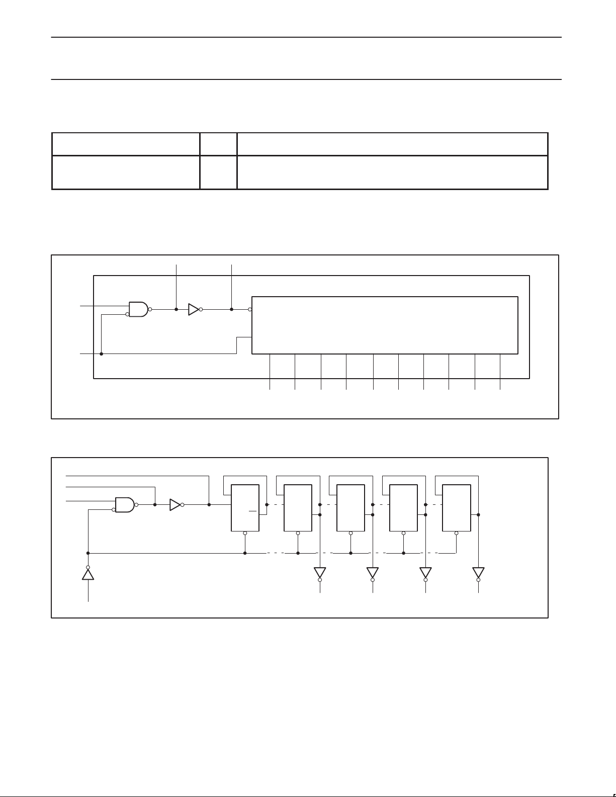
PIN DESCRIPTION
PIN NO. SYMBOL FUNCTION
1, 2, 3 Q11 to Q13 Counter outputs
7, 5, 4, 6,
15, 13, 15
8 GND Ground (0 V)
9 C
10 R
11 RS Clock input/oscillator pin
12 MR Master reset
16 V
PIN CONFIGURATION
Q3 to Q
TC
TC
CC
Q
11
Q
12
Counter outputs
9
External capacitor connection
External resistor connection
Positive supply voltage
1
2
V
16
CC
Q
9
15
LOGIC SYMBOL
11
12
RS
MR
TC
910
CTCR
Q3
Q4
Q5
Q6
Q7
Q8
Q9
Q11
Q12
Q13
SV00307
74LV4060
7
5
4
6
14
13
15
1
2
3
3
Q
13
4
Q
5
5
Q
4
6
Q
6
7
Q
3
GND
89
LOGIC SYMBOL (IEEE/IEC)
9
10
11
12
14
13
12
11
10
SV00308
CX
RX
RCX
CT = 0
CTR14
!G
Q
Q
MR
RS
R
C
+
7
8
TC
TC
CTR14
7
3
5
4
6
CT
14
13
15
9
1
11
2
3
13
11
12
&
CT = 0
+
CT
7
3
5
4
6
14
13
15
9
1
11
2
3
13
1998 Jun 23
(a)
(b)
SV00311
3
Philips Semiconductors Product specification
14-stage binary ripple counter with oscillator
DYNAMIC POWER DISSIPATION
GND = 0 V; T
Total dynamic power dissipation when
using the on–chip oscillator (PD)
NOTE:
1. Where: f
FUNCTIONAL DIAGRAM
11
= 25 C
amb
V
PARAMETER
= output frequency in MHz; f
o
(C
LxVCC
C
= timing capacitance in pF; VCC= supply voltage in V.
t
RS
2
xfo) = sum of the outputs; CL= output load capacitance in pF;
R
TC
CC
(V)
1.2
CPD x f
2.0
CPD x f
3.0
CPD x f
= oscillator frequency in MHz;
osc
910
C
TC
CP
C
osc
osc
osc
D
x V
x V
x V
2
+ (CL x V
CC
2
+ (CL x V
CC
2
+ (CL x V
CC
TYPICAL FORMULA FOR PD (W)
2
x fo) + 2Ct x V
CC
2
x fo) + 2Ct x V
CC
2
x fo) + 2Ct x V
CC
14-stage binary counter
CC
CC
CC
2
x f
2
x f
2
x f
+ 16 x V
osc
+ 460 x V
osc
+ 1000 x V
osc
74LV4060
1
CC
CC
CC
MR
12
LOGIC DIAGRAM
C
TC
R
TC
RS
MR
CP
FF1
C
Q
Q
Q
7
Q
D
4
3
5
Q
5
6
4
6
Q
3
Q
Q
8
7
13
14
Q
9
Q
Q
Q
11
9
1
15
FF14FF12FF10FF4
Q
11
SV00313
Q
12
13
2
3
SV00312
Q
13
1998 Jun 23
4
Philips Semiconductors Product specification
14-stage binary ripple counter with oscillator
TIMING DIAGRAM
RS
MR
Q3
Q4
Q5
Q6
Q7
Q8
74LV4060
4.0962.0481.0245122561286432168421 8.192 16.384
Q9
Q11
Q12
Q13
SV00309
ABSOLUTE MAXIMUM RA TINGS
1, 2
In accordance with the Absolute Maximum Rating System (IEC 134)
Voltages are referenced to GND (ground = 0V)
SYMBOL
V
CC
±I
IK
±I
OK
±I
O
±I
GND
±I
CC
T
stg
P
TOT
DC supply voltage –0.5 to +7.0 V
DC input diode current VI < –0.5 or VI > VCC + 0.5V 20 mA
DC output diode current VO < –0.5 or VO > VCC + 0.5V 50 mA
DC output source or sink current
– standard outputs
DC VCC or GND current for types with
,
–standard outputs
Storage temperature range –65 to +150 °C
Power dissipation per package
–plastic DIL
–plastic mini-pack (SO)
–plastic shrink mini-pack (SSOP and TSSOP)
PARAMETER CONDITIONS RATING UNIT
–0.5V < VO < VCC + 0.5V
25
50
mA
mA
for temperature range: –40 to +125°C
above +70°C derate linearly with 12mW/K
above +70°C derate linearly with 8 mW/K
above +60°C derate linearly with 5.5 mW/K
750
500
400
mW
NOTES:
1. Stresses beyond those listed may cause permanent damage to the device. These are stress ratings only and functional operation of the
device at these or any other conditions beyond those indicated under “recommended operating conditions” is not implied. Exposure to
absolute-maximum-rated conditions for extended periods may affect device reliability .
2. The input and output voltage ratings may be exceeded if the input and output current ratings are observed.
1998 Jun 23
5
Philips Semiconductors Product specification
V
voltage
V
V
voltage
V
V
voltage
V
V
voltage
V
HIGH l
t
R
TC
out ut
14-stage binary ripple counter with oscillator
74LV4060
RECOMMENDED OPERATING CONDITIONS
SYMBOL PARAMETER CONDITIONS MIN TYP. MAX UNIT
V
T
V
amb
tr, t
V
CC
DC supply voltage See Note
Input voltage 0 – V
I
Output voltage 0 – V
O
Operating ambient temperature range in free
air
See DC and AC
characteristics
VCC = 1.0V to 2.0V
Input rise and fall times
f
VCC = 2.0V to 2.7V
VCC = 2.7V to 3.6V
VCC = 3.6V to 5.5V
1
1.0 3.3 5.5 V
CC
CC
–40
–40
–
–
–
–
–
–
–
–
+85
+125
500
200
100
50
NOTES:
1. The LV is guaranteed to function down to V
= 1.0V (input levels GND or VCC); DC characteristics are guaranteed from VCC = 1.2V to VCC = 5.5V.
CC
DC CHARACTERISTICS
Over operating conditions, voltages are referenced to GND (ground = 0 V)
LIMITS
SYMBOL P ARAMETER TEST CONDITIONS
VCC = 1.2V 0.9 – – 0.9 –
IH
HIGH level Input
MR input
VCC = 2.0V 1.4 – – 1.4 –
VCC = 2.7 to 3.6V 2.0 – – 2.0 –
VCC = 4.5 to 5.5V 0.7 * V
VCC = 1.2V – – 0.3 – 0.3
IL
LOW level Input
MR input
VCC = 2.0V – – 0.6 – 0.6
VCC = 2.7 to 3.6V – – 0.8 – 0.8
VCC = 4.5 to 5.5 – – 0.3 * V
VCC = 1.2V 1.0 – – 1.0 –
IH
HIGH level Input
RS input
VCC = 2.0V 1.6 – – 1.6 –
VCC = 2.7 to 3.6V 2.4 – – 2.4 –
VCC = 4.5 to 5.5V 0.8 * V
VCC = 1.2V – – 0.2 – 0.2
IL
LOW level Input
RS input
VCC = 2.0V – – 0.4 – 0.4
VCC = 2.7 to 3.6V – – 0.5 – 0.5
VCC = 4.5 to 5.5 – – 0.2 * V
VCC = 1.2V; RS = GND and MR = GND
–IO = 3.4mA
VCC = 2.0V; RS = GND and MR = GND
V
OH
voltage;
p
evel outpu
–IO = 3.4mA
VCC = 2.7V; RS = GND and MR = GND
–IO = 3.4mA
VCC = 3.0V; RS = GND and MR = GND
–IO = 3.4mA
VCC = 4.5V; RS = GND and MR = GND
–IO = 3.4mA
;
;
;
;
;
-40°C to +85°C -40°C to +125°C
MIN TYP
CC
CC
1
MAX MIN MAX
– – 0.7 * V
CC
– 0.3 * V
– – 0.8 * V
CC
– 0.2 * V
CC
CC
– – – – –
–
–
– – –
– – – – –
2.40 2.82 – 2.20 –
– – – – –
–
CC
–
CC
V
V
°C
ns/V
UNIT
V
1998 Jun 23
6
 Loading...