

Philips 74LV393PW, 74LV393N, 74LV393DB, 74LV393D Datasheet
INTEGRATED CIRCUITS
74LV393
Dual 4-bit binary ripple counter
Product specification
Supersedes data of 1997 Mar 04
IC24 Data Handbook
1997 Jun 10
Philips Semiconductors Product specification
74L V393Dual 4-bit binary ripple counter
FEA TURES
•Optimized for Low Voltage applications: 1.0 to 3.6V
•Accepts TTL input levels between V
•Typical V
T
amb
•Typical V
T
amb
(output ground bounce) 0.8V @ VCC = 3.3V,
OLP
= 25°C
(output VOH undershoot) 2V @ VCC = 3.3V,
OHV
= 25°C
= 2.7V and VCC = 3.6V
CC
•Two 4-bit binary counters with individual clocks
•Divide-by any binary module up to 28 in one package
•Two master resets to clear each 4-bit counter individually
•Output capability: standard
•I
category: MSI
CC
QUICK REFERENCE DATA
GND = 0V; T
SYMBOL
t
PHL/tPLH
f
max
C
I
C
PD
NOTE:
1. C
is used to determine the dynamic power dissipation (PD in µW)
PD
= CPD V
P
D
f
= input frequency in MHz; CL = output load capacity in pF;
i
= output frequency in MHz; VCC = supply voltage in V;
f
o
(C
= 25°C; tr = tf 2.5 ns
amb
CC
2
V
L
fo) = sum of the outputs.
CC
PARAMETER CONDITIONS TYPICAL UNIT
Propagation delay
nCP to nQ
nQ to nQn+1
0
nMR to nQn
Maximum clock frequency 99 MHz
Input capacitance 3.5 pF
Power dissipation capacitance per flip-flop VI = GND to VCC
2
fi (CL V
2
fo) where:
CC
DESCRIPTION
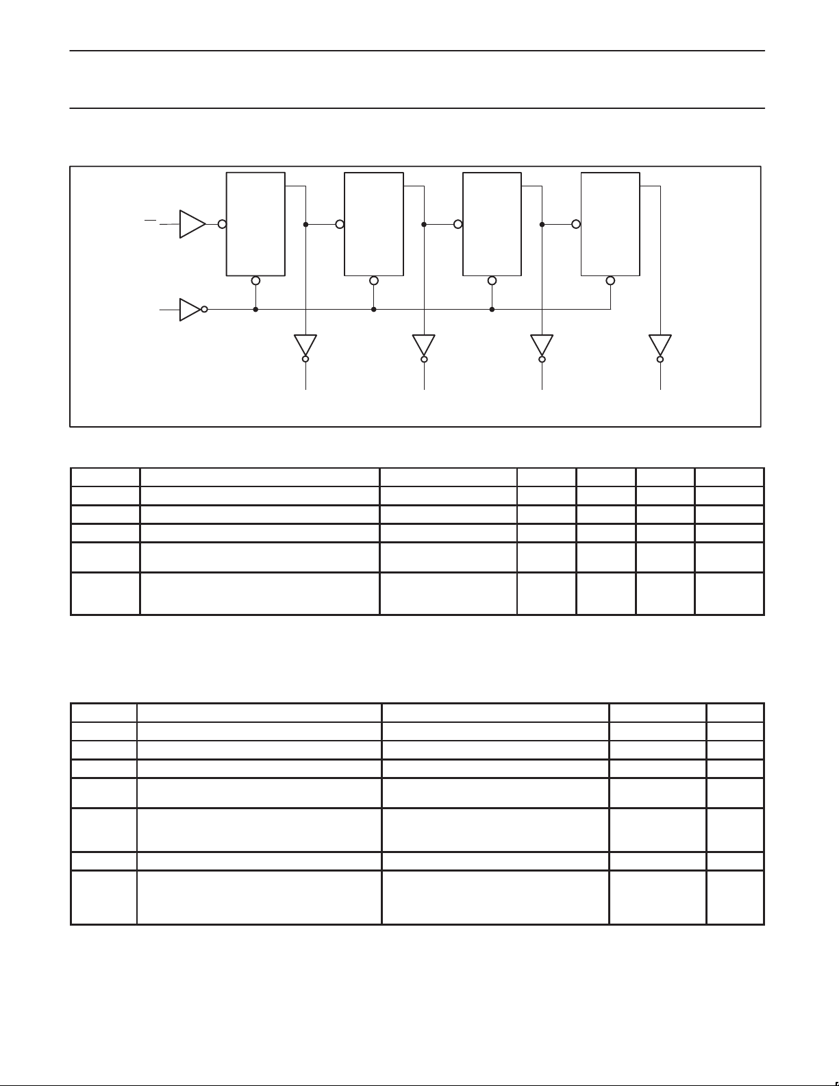
The 74LV393 is a low–voltage Si-gate CMOS device and is pin and
function compatible with 74HC/HCT393.
The 74LV393 is a dual 4-bit binary ripple counter with separate
clocks (1CP
counter.
The operation of each half of the ‘‘393’’ is the same as the ‘‘93’’
except no external clock connections are required. The counters are
triggered by a HIGH-to-LOW transition of the clock inputs. The
counter outputs are internally connected to provide clock inputs to
succeeding stages. The outputs of the ripple counter do not change
synchronously and should not be used for high-speed address
decoding.
The master resets are active-HIGH asynchronous inputs to each
4-bit counter identified by the ‘‘1’’ and ‘‘2’’ in the pin description.
A HIGH level on the nMR input overrides the clock and sets the
outputs LOW.
CL = 15pF
VCC = 3.3V
, 2CP) and master reset (1MR, 2MR) inputs to each
12
4
11
1
23 pF
ns
ORDERING INFORMATION
PACKAGES TEMPERATURE RANGE OUTSIDE NORTH AMERICA NORTH AMERICA PKG. DWG. #
14-Pin Plastic DIL –40°C to +125°C 74LV393 N 74LV393 N SOT27-1
14-Pin Plastic SO –40°C to +125°C 74LV393 D 74LV393 D SOT108-1
14-Pin Plastic SSOP Type II –40°C to +125°C 74LV393 DB 74LV393 DB SOT337-1
14-Pin Plastic TSSOP Type I –40°C to +125°C 74L V393 PW 74LV393PW DH SOT402-1
PIN CONFIGURATION
1
1CP
2
1MR
3
1Q
0
4
1Q
1
5
1Q
2
6
1Q
3
GND
7
1998 Jun 10 853–1936 19545
V
14
2CP
13
2MR
12
2Q
11
2Q
10
2Q
9
2Q
8
SV00672
CC
0
1
2
3
PIN DESCRIPTION
PIN
NUMBER
1, 13 1CP, 2CP
2, 12 1MR, 2MR
3, 4, 5, 6
11, 10, 9, 8
7 GND Ground (0V)
14 V
2
SYMBOL FUNCTION
1Q0 to 1Q
2Q0 to 2Q
CC
3
3
Clock inputs
(HIGH-to-LOW, edge-triggered)
Asynchronous master reset inputs
(active HIGH)
Flip-flop outputs
Positive supply voltage

Philips Semiconductors Product specification
COUNT
74LV393Dual 4-bit binary ripple counter
LOGIC SYMBOL
1
1CP
1
2
1MR
2CP
13
2
12
2MR
LOGIC SYMBOL (IEEE/IEC)
CTR4
2
CT=0
1
+
1Q
1Q
1Q
1Q
2Q
2Q
2Q
2Q
CT
0
1
2
3
0
1
2
3
SV00673
0
3
FUNCTIONAL DIAGRAM
3
4
5
6
11
10
9
8
1CP
211MR
2CP
12132MR
4–BIT
BINARY
RIPPLE
COUNTER
4–BIT
BINARY
RIPPLE
COUNTER
1Q
0
1Q
1
1Q
2
1Q
3
2Q
0
2Q
1
2Q
2
2Q
3
SV00675
3
4
5
6
11
10
9
8
ST ATE DIAGRAM
1
3
4
5
6
0
15
14
3
2
4
5
6
13
11
CTR4
11
0
12
CT=0
13
+
CT
10
9
8
3
COUNT SEQUENCE FOR 1 COUNTER
12
Q
0
10
OUTPUTS
Q
1
9
7
8
SV00676
Q
2
Q
3
0 L L L L
SV00674
1 H L L L
2 L H L L
3 H H L L
4 L L H L
5 H L H L
6 L H H L
7 H H H L
8 L L L H
9 H L L H
10 L H L H
11 H H L H
12 L L H H
13 H L H H
14 L H H H
15 H H H H
1998 Jun 10
3
Philips Semiconductors Product specification
74LV393Dual 4-bit binary ripple counter
LOGIC DIAGRAM
CP
MR
Q
FF1
TTTT
R
D
Q
0
FF2
R
Q
D
Q
1
FF3
R
Q
D
Q
2
FF4
R
D
Q
SV00677
Q
3
RECOMMENDED OPERA TING CONDITIONS
SYMBOL PARAMETER CONDITIONS MIN TYP MAX UNIT
V
CC
V
V
T
amb
tr, t
NOTES:
1. The LV is guaranteed to function down to V
DC supply voltage See Note 1 1.0 3.3 3.6 V
Input voltage 0 – V
I
Output voltage 0 – V
O
Operating ambient temperature range in free
air
Input rise and fall times
f
= 1.0V (input levels GND or VCC); DC characteristics are guaranteed from VCC = 1.2V to VCC =3.6V.
CC
See DC and AC
characteristics
VCC = 1.0V to 2.0V
VCC = 2.0V to 2.7V
VCC = 2.7V to 3.6V
–40
–40
–
–
–
–
–
–
CC
CC
+85
+125
500
200
100
V
V
°C
ns/V
ABSOLUTE MAXIMUM RATINGS
1, 2
In accordance with the Absolute Maximum Rating System (IEC 134).
Voltages are referenced to GND (ground = 0V).
SYMBOL
V
CC
±I
IK
±I
OK
±I
O
±I
GND
±I
CC
T
stg
P
TOT
DC supply voltage –0.5 to +4.6 V
DC input diode current VI < –0.5 or VI > VCC + 0.5V 20 mA
DC output diode current VO < –0.5 or VO > VCC + 0.5V 50 mA
DC output source or sink current
– standard outputs
DC VCC or GND current for types with
,
– standard outputs
Storage temperature range –65 to +150 °C
Power dissipation per package
– plastic DIL
– plastic mini-pack (SO)
– plastic shrink mini-pack (SSOP and TSSOP)
PARAMETER CONDITIONS RATING UNIT
–0.5V < VO < VCC + 0.5V 25 mA
50 mA
for temperature range: –40 to +125°C
above +70°C derate linearly with 12 mW/K
above +70°C derate linearly with 8 mW/K
above +60°C derate linearly with 5.5 mW/K
750
500
400
mW
NOTES:
1. Stresses beyond those listed may cause permanent damage to the device. These are stress ratings only and functional operation of the
device at these or any other conditions beyond those indicated under “recommended operating conditions” is not implied. Exposure to
absolute-maximum-rated conditions for extended periods may affect device reliability .
2. The input and output voltage ratings may be exceeded if the input and output current ratings are observed.
1998 Jun 10
4
 Loading...