

Philips 74LV374N, 74LV374DB, 74LV374D, 74LV374PW Datasheet
74LV374
Octal D-type flip-flop;
positive edge-trigger (3-State)
Product specification
Supersedes data of 1996 Feb
IC24 Data Handbook
1997 Mar 20
INTEGRATED CIRCUITS
Philips Semiconductors Product specification
74L V374
Octal D-type flip-flop; positive edge-trigger (3-State)
2
1997 Mar 20
FEATURES
•Wide operating voltage: 1.0 to 5.5V
•Optimized for Low Voltage applications: 1.0 to 3.6V
•Accepts TTL input levels between V
CC
= 2.7V and VCC = 3.6V
•Typical V
OLP
(output ground bounce) 0.8V @ VCC = 3.3V ,
T
amb
= 25°C
•Typical V
OHV
(output VOH undershoot) 2V @ VCC = 3.3V ,
T
amb
= 25°C
•Common 3-State output enable input
•Output capability: bus driver
•I
CC
category: MSI
DESCRIPTION
The 74LV374 is a low-voltage Si-gate CMOS device and is pin and
function compatible with 74HC/HCT374.
The 74LV374 is an octal D-type flip–flop featuring separate D-type
inputs for each flip-flop and 3-state outputs for bus oriented
applications. A clock (CP) and an output enable (OE
) input are
common to all flip-flops.
The eight flip-flops will store the state of their individual D-inputs that
meet the set-up and hold times requirements on the LOW-to-HIGH
CP transition.
When OE
is LOW, the contents of the eight flip-flops is available at
the outputs. When OE
is HIGH, the outputs go to the high
impedance OFF-state. Operation of the OE
input does not affect the
state of the flip-flops.
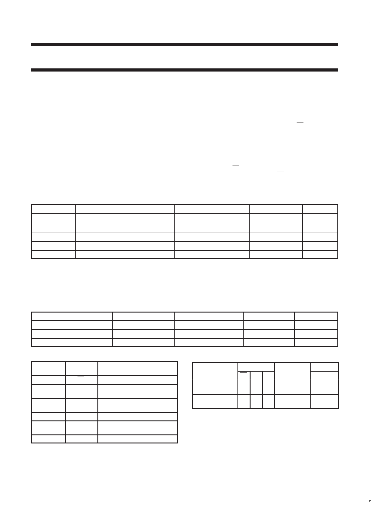
QUICK REFERENCE DA TA
GND = 0V; T
amb
= 25°C; tr =tf 2.5 ns
SYMBOL
PARAMETER CONDITIONS TYPICAL UNIT
t
PHL/tPLH
Propagation delay
CP to Q
n
CL = 15pF
VCC = 3.3V
14 ns
f
max
Maximum clock frequency 77 MHz
C
I
Input capacitance 3.5 pF
C
PD
Power dissipation capacitance per flip-flop Notes 1 and 2 25 pF
NOTES:
1. C
PD
is used to determine the dynamic power dissipation (PD in µW)
P
D
= CPD V
CC
2
x fi (CL V
CC
2
fo) where:
f
i
= input frequency in MHz; CL = output load capacity in pF;
f
o
= output frequency in MHz; VCC = supply voltage in V;
(C
L
V
CC
2
fo) = sum of the outputs.
2. The condition is V
I
= GND to V
CC
ORDERING INFORMATION
PACKAGES TEMPERATURE RANGE OUTSIDE NORTH AMERICA NORTH AMERICA PKG. DWG. #
20-Pin Plastic DIL –40°C to +125°C 74LV374 N 74LV374 N SOT146-1
20-Pin Plastic SO –40°C to +125°C 74LV374 D 74LV374 D SOT163-1
20-Pin Plastic SSOP Type II –40°C to +125°C 74LV374 DB 74LV374 DB SOT339-1
PIN DESCRIPTION
PIN
NUMBER
SYMBOL FUNCTION
1 OE Output enable input (active-LOW)
2, 5, 6, 9, 12,
15, 16, 19
Q0 to Q7 3-State flip-flop outputs
3, 4, 7, 8, 13,
14, 17, 18
D0 to D7 Data inputs
10 GND Ground (0V)
11 CP
Clock input (LOW-to-HIGH, edgetriggered)
20 V
CC
Positive supply voltage
FUNCTION TABLE
OPERATING
INPUTS
INTERNAL
OUTPUTS
MODES
OE CP Dn
FLIP-FLOPS
Q0 to Q7
Load and read
register
LL↑↑l
h
L
H
L
H
Load register and
disable outputsHH↑↑lh
L
H
Z
Z
H = HIGH voltage level
h = HIGH voltage level one set-up time prior to the
LOW-to-HIGH CP transition
L = LOW voltage level
l = LOW voltage level one set-up time prior to the
LOW-to-HIGH CP transition
Z = High impedance OFF-state
↑ = LOW–to–HIGH clock transition

Philips Semiconductors Product specification
74LV374
Octal D-type flip-flop; positive edge-trigger (3-State)
1997 Mar 20
3
PIN CONFIGURATION
1
2
3
4
5
6
7
8
9
10 11
12
13
14
15
16
17
18
19
20OE
Q0
D0
D1
Q1
Q2
D2
D3
Q3
GND
V
CC
Q7
D7
D6
Q6
Q5
D5
D4
Q4
CP
SV00338
LOGIC SYMBOL (IEEE/IEC)
11
1
C1
EN1
1D
3
4
7
8
13
14
17
18
2
5
6
9
12
15
16
19
SV00340
LOGIC SYMBOL
CP
D0
D1
D2
D3
D4
D5
D6
D7
Q0
Q1
Q2
Q3
Q4
Q5
Q6
Q7
2
5
6
9
12
15
16
19
3
4
7
8
13
14
17
18
11
SV00339
1
OE
FUNCTIONAL DIAGRAM
SV00341
3
4
76
5
2
89
13 12
14 15
17 16
18 19
11
1
D
0
D
1
D
2
D
3
D
4
D
5
D
6
D
7
CP
OE
Q
0
Q
1
Q
2
Q
3
Q
4
Q
5
Q
6
Q
7
FF1
to
FF8
3-STATE
OUTPUTS
LOGIC DIAGRAM
SV00342
D
D0
Q0
D1 D2 D3 D4 D5 D6 D7
Q1 Q2 Q3 Q4 Q5 Q6 Q7
CP
OE
Q
CP
D Q
CP
D Q
CP
D Q
CP
D Q
CP
D Q
CP
D Q
CP
D Q
CP
FF1 FF2 FF3 FF4 FF5 FF6 FF7 FF8
Philips Semiconductors Product specification
74LV374
Octal D-type flip-flop; positive edge-trigger (3-State)
1997 Mar 20
4
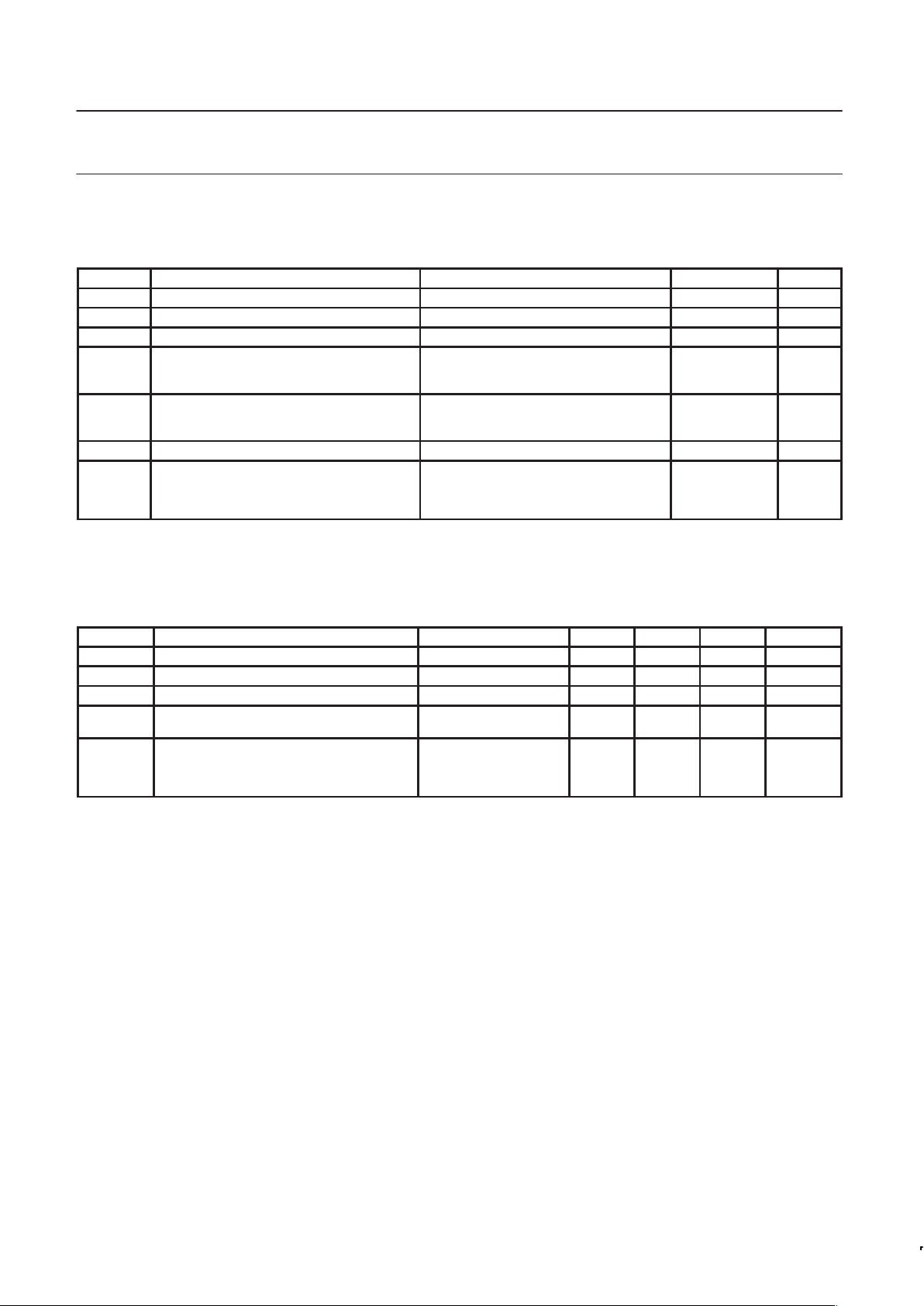
ABSOLUTE MAXIMUM RATINGS
1, 2
In accordance with the Absolute Maximum Rating System (IEC 134)
Voltages are referenced to GND (ground = 0V)
SYMBOL
PARAMETER CONDITIONS RATING UNIT
V
CC
DC supply voltage –0.5 to +7.0 V
±I
IK
DC input diode current VI < –0.5 or VI > VCC + 0.5V 20 mA
±I
OK
DC output diode current VO < –0.5 or VO > VCC + 0.5V 50 mA
±I
O
DC output source or sink current
– standard outputs
– bus driver outputs
–0.5V < VO < VCC + 0.5V
25
35
mA
±I
GND
,
±I
CC
DC VCC or GND current for types with
–standard outputs
–bus driver outputs
50
70
mA
T
stg
Storage temperature range –65 to +150 °C
P
TOT
Power dissipation per package
–plastic DIL
–plastic mini-pack (SO)
–plastic shrink mini-pack (SSOP and TSSOP)
for temperature range: –40 to +125°C
above +70°C derate linearly with 12mW/K
above +70°C derate linearly with 8 mW/K
above +60°C derate linearly with 5.5 mW/K
750
500
400
mW
NOTES:
1. Stresses beyond those listed may cause permanent damage to the device. These are stress ratings only and functional operation of the
device at these or any other conditions beyond those indicated under “recommended operating conditions” is not implied. Exposure to
absolute-maximum-rated conditions for extended periods may affect device reliability .
2. The input and output voltage ratings may be exceeded if the input and output current ratings are observed.
RECOMMENDED OPERATING CONDITIONS
SYMBOL PARAMETER CONDITIONS MIN TYP. MAX UNIT
V
CC
DC supply voltage See Note1 1.0 3.3 5.5 V
V
I
Input voltage 0 – V
CC
V
V
O
Output voltage 0 – V
CC
V
T
amb
Operating ambient temperature range in free
air
See DC and AC
characteristics per device
–40
–40
+85
+125
°C
tr, t
f
Input rise and fall times except for
Schmitt-trigger inputs
VCC = 1.0V to 2.0V
VCC = 2.0V to 2.7V
VCC = 2.7V to 3.6V
VCC = 3.6V to 5.5V
–
–
–
–
–
–
–
500
200
100
50
ns/V
NOTES:
1. The LV is guaranteed to function down to V
CC
= 1.0V (input levels GND or VCC); DC characteristics are guaranteed from VCC = 1.2V to VCC = 5.5V.
 Loading...