

Philips 74LV273PW, 74LV273N, 74LV273D Datasheet

INTEGRATED CIRCUITS
74LV273
Octal D-type flip-flop with reset;
positive-edge trigger
Product specification
Supersedes data of 1997 Apr 07
IC24 Data Handbook
1998 May 29

Philips Semiconductors Product specification
Octal D-type flip-flop with reset; positive edge-trigger
FEA TURES
•Wide operating voltage: 1.0 to 5.5V
•Optimized for Low Voltage applications: 1.0 to 3.6V
•Accepts TTL input levels between V
•Typical V
T
amb
•Typical V
T
amb
(output ground bounce) 0.8V @ VCC = 3.3V,
OLP
= 25°C
(output VOH undershoot) 2V @ VCC = 3.3V,
OHV
= 25°C
= 2.7V and VCC = 3.6V
CC
•Ideal buffer for MOS microprocessor or memory
•Common clock and master reset
•Output capability: standard
•I
category: MSI
CC
QUICK REFERENCE DATA
GND = 0V; T
SYMBOL
t
PHL/tPLH
f
max
C
I
C
PD
NOTES:
is used to determine the dynamic power dissipation (PD in µW)
1. C
PD
P
= CPD V
D
= input frequency in MHz; CL = output load capacitance in pF;
f
i
f
= output frequency in MHz; VCC = supply voltage in V;
o
(C
2. The condition is V
= 25°C; tr =tf 2.5 ns
amb
CC
2
V
L
fo) = sum of the outputs.
CC
PARAMETER CONDITIONS TYPICAL UNIT
Propagation delay
CP to Q
n;
MR to Q
n
Maximum clock frequency 110 MHz
Input capacitance 3.5 pF
Power dissipation capacitance per flip-flop Notes 1 and 2 20 pF
2
x fi (CL V
= GND to V
I
CC
2
fo) where:
CC
DESCRIPTION
The 74LV273 is a low-voltage Si-gate CMOS device and is pin and
function compatible with the 74HC/HCT273.
The 74LV273 has eight edge-triggered , D-type flip-flops with
individual D inputs and Q outputs. The common clock (CP) and
master reset (MR
simultaneously . The state of each D input, one set-up time before
the LOW-to-HIGH clock transition, is transferred to the
corresponding output (Qn) of the flip-flop.
All outputs will be forced LOW independently of clock or data inputs
by a LOW voltage level on the MR
The device is useful for applications where the true output only is
required and the clock and master reset are common to all storage
elements.
CL = 15pF
VCC = 3.3V
) inputs load and reset (clear) all flip-flops
input.
12
13
74L V273
ns
ORDERING INFORMATION
PACKAGES TEMPERATURE RANGE OUTSIDE NORTH AMERICA NORTH AMERICA PKG. DWG. #
20-Pin Plastic DIL –40°C to +125°C 74LV273 N 74LV273 N SOT146-1
20-Pin Plastic SO –40°C to +125°C 74LV273 D 74LV273 D SOT163-1
20-Pin Plastic SSOP Type II –40°C to +125°C 74LV273 DB 74LV273 DB SOT339-1
20-Pin Plastic TSSOP –40°C to +125°C 74LV273 PW 74LV273PW DH SOT360-1
1998 May 29 853–1965 19466
2
Philips Semiconductors Product specification
Octal D-type flip-flop with reset; positive edge-trigger
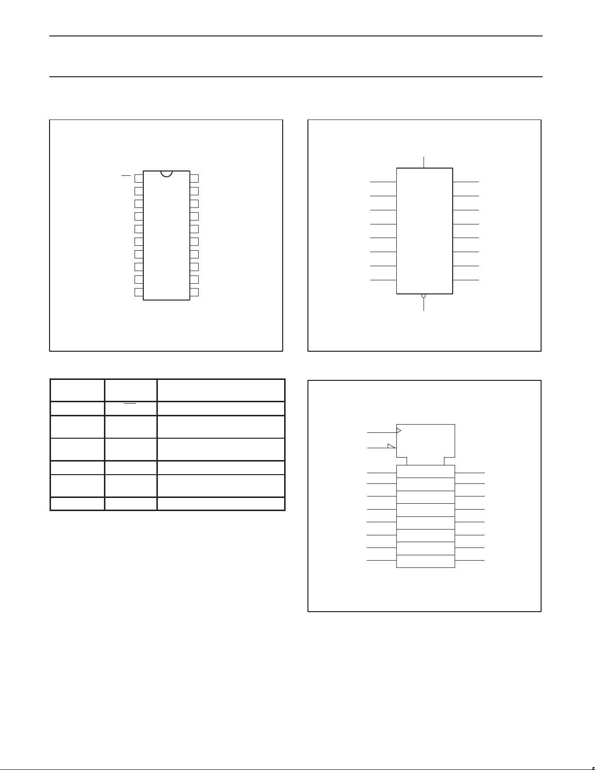
PIN CONFIGURATION
1
MR
Q
2
0
3
D
0
4
D
1
5
Q
1
6
Q
2
7
D
2
8
D
3
9
Q
3
10 11
GND
V
20
CC
Q
19
7
18
D
7
17
D
6
16
Q
6
15
Q
5
14
D
5
13
D
4
12
Q
4
CP
LOGIC SYMBOL
74LV273
11
3
4
7
8
13
14
17
18
CP
MR
Q
0
Q
1
Q
2
Q
3
Q
4
Q
5
Q
6
Q
7
1
D
0
D
1
D
2
D
3
D
4
D
5
D
6
D
7
2
5
6
9
12
15
16
19
SV00366
PIN DESCRIPTION
PIN
NUMBER
1 MR Master reset input (active-LOW)
2, 5, 6, 9, 12,
15, 16, 19
3, 4, 7, 8, 13,
14, 17, 18
10 GND Ground (0V)
11 CP
20 V
SYMBOL FUNCTION
Q0 to Q
D0 to D
Flip-flop outputs
7
Data inputs
7
Clock input (LOW-to-HIGH, edgetriggered)
CC
Positive supply voltage
LOGIC SYMBOL (IEEE/IEC)
11
1
3
4
7
89
13
14
17 16
18
C1
R
1D
SV00367
2
5
6
12
15
19
SV00368
1998 May 29
3

Philips Semiconductors Product specification
OPERATING MODES
Octal D-type flip-flop with reset; positive edge-trigger
FUNCTIONAL DIAGRAM
3
D
0
4
D
1
D
76
2
8D
3
13 12
D
4
14 15
D
5
17 D
6
18 19D
7
1
MR
11
CP
FF0
FF7
2
Q
0
5
Q
1
Q
2
Q
9
3
to
Q
4
Q
5
16
Q
6
Q
7
FUNCTION TABLE
Reset (clear) L X X L
Load (‘1’) H ↑ h H
Load (‘0’) H ↑ l L
H = HIGH voltage level
h = HIGH voltage level one set-up time prior to the
LOW-to-HIGH CP transition
L = LOW voltage level
l = LOW voltage level one set-up time prior to the
LOW-to-HIGH CP transition
↑ = LOW–to–HIGH clock transition
X = Don’t care
74LV273
INPUTS OUTPUTS
MR CP D
n
Q0 to Q
7
SV00369
RECOMMENDED OPERATING CONDITIONS
SYMBOL PARAMETER CONDITIONS MIN TYP. MAX UNIT
V
CC
V
V
T
amb
tr, t
NOTES:
1. The LV is guaranteed to function down to V
DC supply voltage See Note1 1.0 3.3 5.5 V
Input voltage 0 – V
I
Output voltage 0 – V
O
Operating ambient temperature range in free
air
Input rise and fall times
f
= 1.0V (input levels GND or VCC); DC characteristics are guaranteed from VCC = 1.2V to VCC = 5.5V.
CC
See DC and AC
characteristics
VCC = 1.0V to 2.0V
VCC = 2.0V to 2.7V
VCC = 2.7V to 3.6V
VCC = 3.6V to 5.5V
–40
–40
–
–
–
–
–
–
–
CC
CC
+85
+125
500
200
100
50
V
V
°C
ns/V
1998 May 29
4
 Loading...