

Philips 74LV251PW, 74LV251N, 74LV251DB, 74LV251D Datasheet

INTEGRATED CIRCUITS
74LV251
8-input multiplexer (3-State)
Product specification
Supersedes data of 1997 Apr 10
IC24 Data Handbook
1998 May 20

Philips Semiconductors Product specification
74L V2518-input multiplexer (3-State)
FEA TURES
•Optimized for low voltage applications: 1.0 to 3.6 V
•Accepts TTL input levels between V
•Typical V
T
amb
•Typical V
T
amb
(output ground bounce) < 0.8 V at V
OLP
= 25°C
(output VOH undershoot) > 2 V at V
OHV
= 25°C
= 2.7 V and V
CC
CC
CC
CC
= 3.3 V,
= 3.3 V,
•True and complement outputs
•Both outputs are 3-State for further multiplexer expansion
•Multifunction capability
•Permits multiplexing from n-lines to one line
•Output capability: standard
•I
category: MSI
CC
QUICK REFERENCE DATA
GND = 0 V; T
SYMBOL
t
PHL/tPLH
C
I
C
PD
NOTE:
1. C
is used to determine the dynamic power dissipation (PD in µW)
PD
= CPD × V
P
D
f
= input frequency in MHz; CL = output load capacitance in pF;
i
= output frequency in MHz; VCC = supply voltage in V;
f
o
(C
L
= 25°C; tr = t
amb
Propagation delay
In to Y
In to Y
Sn to Y
S
to Y
n
Input capacitance 3.5 pF
Power dissipation capacitance per gate
2
× fi (CL × V
CC
2
× V
× fo) = sum of the outputs.
CC
≤ 2.5 ns
f
PARAMETER CONDITIONS TYPICAL UNIT
2
× fo) where:
CC
= 3.6 V
CL = 15 pF;
VCC = 3.3 V
VCC = 3.3 V
VI = GND to V
DESCRIPTION
The 74LV251 is a low-voltage Si-gate CMOS device and is pin and
function compatible with 74HC/HCT251.
The 74LV251 is an 8-input multiplexer with 8 binary inputs (I
output enable input (OE
the eight binary inputs is selected by the select inputs and is routed to
the outputs (Y, Y). Both outputs are in the high impedance OFF-state
(Z) when the output enable input is HIGH, allowing multiplexer
expansion by tying the outputs.
1
CC
) and three select inputs (S0, S1, S2). One of
14
16
19
20
44 pF
to I7), an
0
ns
ORDERING INFORMATION
PACKAGES TEMPERATURE RANGE OUTSIDE NORTH AMERICA NORTH AMERICA PKG. DWG. #
16-Pin Plastic DIL –40°C to +125°C 74LV251 N 74LV251 N SOT38-4
16-Pin Plastic SO –40°C to +125°C 74LV251 D 74LV251 D SOT109-1
16-Pin Plastic SSOP Type II –40°C to +125°C 74L V251 DB 74LV251 DB SOT338-1
16-Pin Plastic TSSOP Type I –40°C to +125°C 74LV251 PW 74LV251PW DH SOT403-1
1998 May 20 853–1967 19420
2

Philips Semiconductors Product specification
74LV2518-input multiplexer (3-State)
PIN CONFIGURATION
1
I
3
2
I
2
3
I
1
4
I
0
5
Y
6
Y
7
QE
8
GND
LOGIC SYMBOL
S0 S1 S2
4
3
2
1
15
14
13
12
I
0
I
1
I
2
I
3
I
4
I
5
I
6
I
7
11 10 9
OE
7
Y
Y
16
15
14
13
12
11
10
9
SV00629
SV00630
PIN DESCRIPTION
V
CC
I
4
I
5
I
6
I
7
S
0
S
1
S
2
PIN
NUMBER
4, 3, 2, 1, 15,
14, 13, 12
5 Y Multiplexer output
6 Y Complementary multiplexer output
7 OE
8 GND Ground (0 V)
11, 10, 9 S0 to S2Select inputs
16 V
SYMBOL FUNCTION
I0 to I
Multiplexer inputs
7
3-State output enable input (active
LOW)
CC
Positive supply voltage
LOGIC SYMBOL (IEEE/IEC)
MUX
7
EN
11
10
5
6
15
14
13
12
0
0
G
9
4
3
2
1
7
2
0
1
2
3
4
5
6
7
5
6
SV00631
FUNCTIONAL DIAGRAM
4 3 2 1 15 14 13 12
I1I2I3I4I5I6I
I
0
S
11
0
S
10
S
9
OE
7
1998 May 20
1
2
MULTIPLEXER
7
Y
6
Y
5
SV00632
3
Philips Semiconductors Product specification
74LV2518-input multiplexer (3-State)
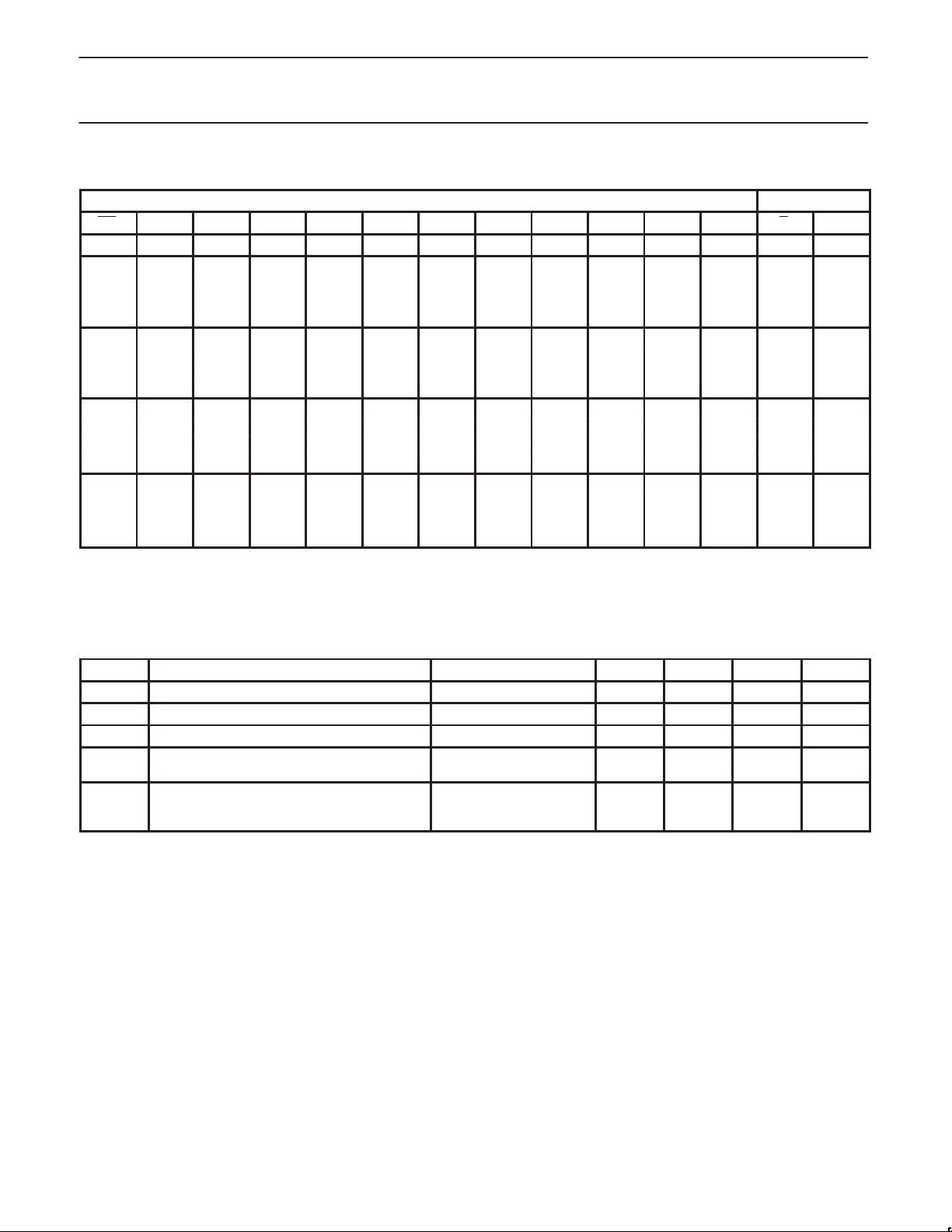
FUNCTION TABLE
INPUTS OUTPUTS
OE S
2
H X X X X X X X X X X X Z Z
L L L L L X X X X X X X H L
L L L L H X X X X X X X L H
L L L H X L X X X X X X H L
L L L H X H X X X X X X L H
L L H L X X L X X X X X H L
L L H L X X H X X X X X L H
L L H H X X X L X X X X H L
L L H H X X X H X X X X L H
L H L L X X X X L X X X H L
L H L L X X X X H X X X L H
L H L H X X X X X L X X H L
L H L H X X X X X H X X L H
L H H L X X X X X X L X H L
L H H L X X X X X X H X L H
L H H H X X X X X X X L H L
L H H H X X X X X X X H L H
NOTES:
H = HIGH voltage level
L = LOW voltage level
X = don’t care
Z = high impedance OFF-state
S
1
S
0
I
0
I
1
I
2
I
3
I
4
I
5
I
6
I
7
Y Y
RECOMMENDED OPERATING CONDITIONS
SYMBOL PARAMETER CONDITIONS MIN TYP MAX UNIT
V
V
V
T
amb
tr, t
NOTE:
1. The LV is guaranteed to function down to V
DC supply voltage See Note 1 1.0 3.3 3.6 V
CC
Input voltage 0 – V
I
Output voltage 0 – V
O
Operating ambient temperature range in free air
Input rise and fall times
f
CC
See DC and AC
characteristics
VCC = 1.0V to 2.0V
VCC = 2.0V to 2.7V
VCC = 2.7V to 3.6V
= 1.0V (input levels GND or VCC); DC characteristics are guaranteed from VCC = 1.2V to VCC = 5.5V.
–40
–40
–
–
–
–
–
–
CC
CC
+85
+125
500
200
100
ns/V
V
V
°C
1998 May 20
4
 Loading...