

Philips 74LV165PW, 74LV165N, 74LV165DB, 74LV165D Datasheet
INTEGRATED CIRCUITS
74LV165
8-bit parallel-in/serial-out shift register
Product specification
Supersedes data of 1997 May 15
IC24 Data Handbook
1998 May 07
Philips Semiconductors Product specification
74L V1658-bit parallel-in/serial-out shift register
FEA TURES
•Wide operating voltage: 1.0 to 5.5 V
•Optimized for low voltage applications: 1.0 to 3.6 V
•Accepts TTL input levels between V
•Typical V
T
amb
•Typical V
T
amb
(output ground bounce) < 0.8 V at V
OLP
= 25°C
(output VOH undershoot) > 2 V at V
OHV
= 25°C
= 2.7 V and V
CC
•Asynchronous 8-bit parallel load
•Synchronous serial input
•Output capability: standard
•I
category: MSI
CC
CC
CC
= 3.6 V
CC
= 3.3 V,
= 3.3 V,
DESCRIPTION
The 74LV165 is a low-voltage Si-gate CMOS device and is pin and
function compatible with 74HC/HCT165.
The 74LV165 is an 8-bit parallel-load or serial-in shift register with
complementary serial outputs (Q
stage. When the parallel load (PL
D
to D7 inputs are loaded into the register asynchronously. When PL
0
is HIGH, data enters the register serially at the DS input and shifts one
place to the right (Q
transition. This feature allows parallel-to-serial converter expansion by
tying the Q
7
0→Q1→Q2
output to the DS input of the succeeding stage.
The clock input is a gated-OR structure which allows one input to be
used as an active LOW clock enable (CE
for the CP and CE
inputs is arbitrary and can be reversed for layout
convenience. The LOW-to-HIGH transition of input CE
take place while CP HIGH for predictable operation. Either the CP or
the CE
should be HIGH before the LOW-to-HIGH transition of PL to
prevent shifting the data when PL
and Q7) available from the last
7
) input is LOW, parallel data from the
, etc.) with each positive-going clock
) input. The pin assignment
should only
is activated.
QUICK REFERENCE DATA
GND = 0 V; T
= 25°C; tr = t
amb
SYMBOL
Propagation delay
t
PHL/tPLH
CE, CP to Q7, Q
PL to Q7, Q
D7 to Q7, Q
f
C
C
max
I
PD
Maximum clock frequency 78 MHz
Input capacitance 3.5 pF
Power dissipation capacitance per gate
NOTES:
is used to determine the dynamic power dissipation (PD in µW)
1. C
PD
P
= CPD × V
D
f
= input frequency in MHz; CL = output load capacitance in pF;
i
= output frequency in MHz; VCC = supply voltage in V;
f
o
(C
× V
L
2
× fi (CL × V
CC
2
× fo) = sum of the outputs.
CC
≤ 2.5 ns
f
PARAMETER CONDITIONS TYPICAL UNIT
CL = 15 pF;
7
7
7
2
× fo) where:
CC
VCC = 3.3 V
V
= 3.3 V
CC
VI = GND to V
CC
1
18
18
14
35 pF
ns
ORDERING INFORMATION
PACKAGES TEMPERATURE RANGE OUTSIDE NORTH AMERICA NORTH AMERICA PKG. DWG. #
16-Pin Plastic DIL –40°C to +125°C 74LV165 N 74LV165 N SOT38-4
16-Pin Plastic SO –40°C to +125°C 74LV165 D 74LV165 D SOT109-1
16-Pin Plastic SSOP Type II –40°C to +125°C 74LV165 DB 74LV165 DB SOT338-1
16-Pin Plastic TSSOP Type I –40°C to +125°C 74LV165 PW 74LV165PW DH SOT403-1
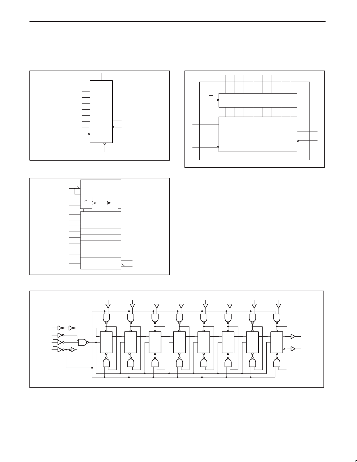
PIN CONFIGURATION
1
PL
2
CP
3
D
4
4
D
5
5
D
6
6
D
7
7
Q
7
8
GND
1998 May 07 853–1915 19349
16
15
14
13
12
11
10
9
SV00585
V
CE
D
D
D
D
D
Q
CC
3
2
1
0
S
7
PIN DESCRIPTION
PIN NUMBER SYMBOL FUNCTION
1
2 CP
7 Q
8 GND Ground (0 V)
9 Q
10 D
11, 12, 13, 14, 3, 4, 5, 6 D0 to D7Parallel data inputs
15 CE
16 V
2
PL Asynchronous parallel load
input (active LOW)
Clock input (LOW to
HIGH, edge-triggered)
7
7
S
Complementary output from
the last stage
Serial output from last stage
Serial data input
Clock enable input
(active LOW)
CC
Positive supply voltage
Philips Semiconductors Product specification
8-bit parallel-in/serial-out shift register
LOGIC SYMBOL
10
D
S
D
11
0
12
D
1
13
D
2
14
D
3
3
D
4
4
D
5
5
D
6
6
D
7
1
PL
CP
215
LOGIC SYMBOL (IEEE/IEC)
1
15
2
10
11
12
13
14
3
4
5
6
SRG8
C2 [LOAD]
G1 [SHIFT]
>
1
1
3D
2D
2D
C3/
CE
Q
7
Q
7
SV00586
9
7
9
7
SV00587
FUNCTIONAL DIAGRAM
D
1
PL
D
10
15
S
2
CP
CE
D2D
0
1
8–BIT SHIFT REGISTER
PARALLEL– IN / SERIAL – OUT
74LV165
654314131211
D
D
3
D6D
D
5
4
7
9
Q
7
7
Q
7
SV00588
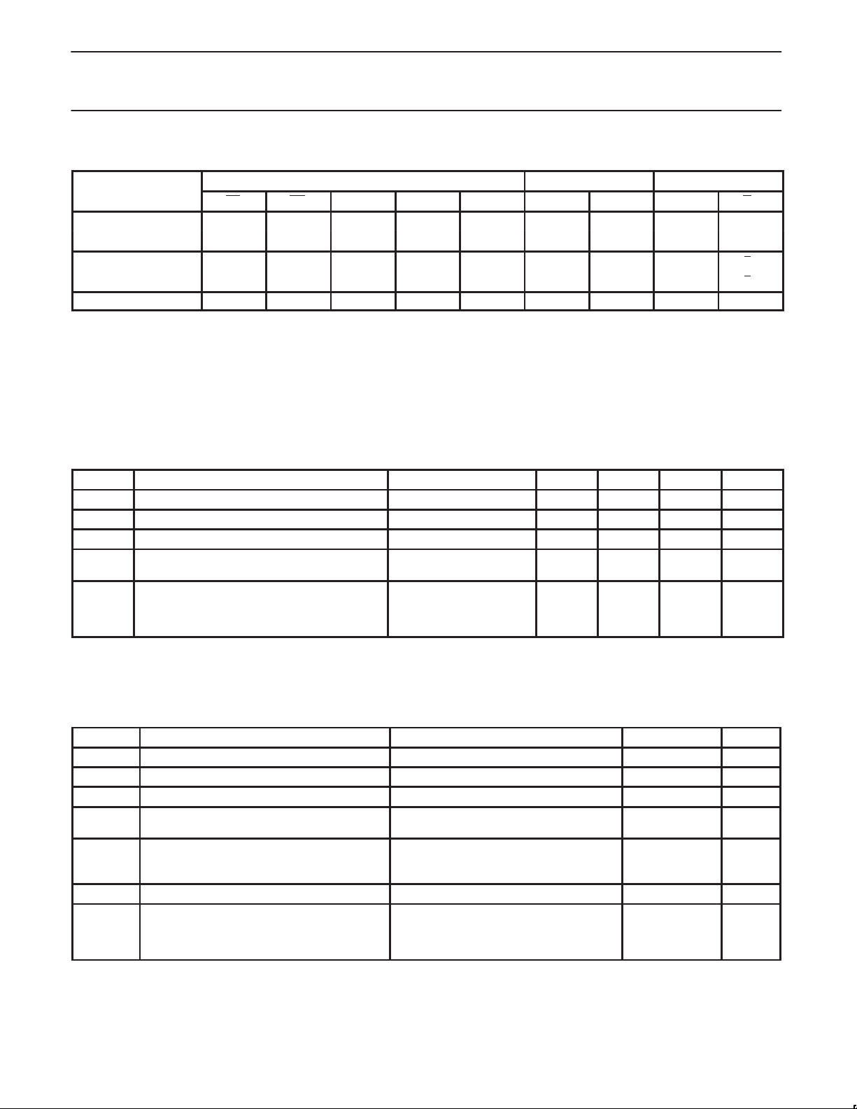
LOGIC DIAGRAM
D
S
CP
CE
PL
1998 May 07
D
0
S
D
Q
D
CP
FF0 FF1 FF2 FF3 FF4 FF5 FF6 FF7
R
D
D
1
S
D
Q
D
CP
R
D
D
2
S
D
Q
D
CP
R
D
D
3
S
D
Q
D
CP
R
D
D
4
S
D
Q
D
CP
R
D
D
5
S
D
Q
D
CP
R
D
D
6
S
D
Q
D
CP
R
D
3
D
7
S
D
D
CP
R
D
Q
Q
Q
7
Q
7
SV00589
Philips Semiconductors Product specification
OPERATING MODES
Parallel load
Serial Shift
8-bit parallel-in/serial-out shift register
74LV165
FUNCTION TABLE
INPUTS Qn REGISTERS OUTPUTS
PL CE CP D
S
D0–D
7
Q
0
Q1–Q
6
Q
7
L X X X L L L–L L H
L X X X H H H–H H L
H L ↑ l X L q0–q
H L ↑ h X H q0–q
Hold “do nothing” H H X X X q
5
5
0
q1–q
6
q
6
q
6
q
7
NOTES:
H = HIGH voltage level
h = HIGH voltage level one set-up time prior to the LOW-to-HIGH clock transition
L = LOW voltage level
I = LOW voltage level level one set-up time prior to the LOW-to-HIGH clock transition
q = lower case letters indicate the state of the referenced output one set-up time prior to the LOW-to-HIGH clock transition
X = don’t care
↑ = LOW-to-HIGH clock transition
RECOMMENDED OPERATING CONDITIONS
SYMBOL PARAMETER CONDITIONS MIN TYP MAX UNIT
V
V
V
T
amb
tr, t
NOTE:
1. The LV is guaranteed to function down to V
DC supply voltage See Note 1 1.0 3.3 5.5 V
CC
Input voltage 0 – V
I
Output voltage 0 – V
O
Operating ambient temperature range in free air
Input rise and fall times
f
CC
See DC and AC
characteristics
VCC = 1.0V to 2.0V
VCC = 2.0V to 2.7V
VCC = 2.7V to 3.6V
VCC = 3.6V to 5.5V
= 1.0V (input levels GND or VCC); DC characteristics are guaranteed from VCC = 1.2V to VCC = 5.5V.
–40
–40
–
–
–
–
–
–
–
–
CC
CC
+85
+125
500
200
100
50
ns/V
Q
q
q
q
°C
7
6
6
7
V
V
ABSOLUTE MAXIMUM RATINGS
In accordance with the Absolute Maximum Rating System (IEC 134).
Voltages are referenced to GND (ground = 0 V).
SYMBOL
V
I
I
I
I
I
T
P
NOTES:
1. Stresses beyond those listed may cause permanent damage to the device. These are stress ratings only and functional operation of the
device at these or any other conditions beyond those indicated under “recommended operating conditions” is not implied. Exposure to
absolute-maximum-rated conditions for extended periods may affect device reliability .
2. The input and output voltage ratings may be exceeded if the input and output current ratings are observed.
1998 May 07
CC
IK
OK
O
GND
CC
stg
TOT
1, 2
PARAMETER CONDITIONS RATING UNIT
DC supply voltage –0.5 to +7.0 V
DC input diode current VI < –0.5 or VI > VCC + 0.5V 20 mA
DC output diode current VO < –0.5 or VO > VCC + 0.5V 50 mA
DC output source or sink current
– standard outputs
DC VCC or GND current for types with
,
– standard outputs 50
–0.5V < VO < VCC + 0.5V
25
Storage temperature range –65 to +150 °C
Power dissipation per package
– plastic DIL
– plastic mini-pack (SO)
– plastic shrink mini-pack (SSOP and TSSOP)
for temperature range: –40 to +125°C
above +70°C derate linearly with 12 mW/K
above +70°C derate linearly with 8 mW/K
above +60°C derate linearly with 5.5 mW/K
750
500
400
4
mA
mA
mW

Philips Semiconductors Product specification
V
V
V
V
voltage all out uts
g
V
g
V
voltage all out uts
g
V
g
V
8-bit parallel-in/serial-out shift register
DC ELECTRICAL CHARACTERISTICS
Over recommended operating conditions. V oltages are referenced to GND (ground = 0 V).
SYMBOL P ARAMETER TEST CONDITIONS
VCC = 1.2 V 0.9 0.9
IH
HIGH level Input
voltage
VCC = 2.0 V 1.4 1.4
VCC = 2.7 to 3.6 V 2.0 2.0
VCC = 4.5 to 5.5 V 0.7V
VCC = 1.2 V 0.3 0.3
IL
LOW level Input
voltage
VCC = 2.0 V 0.6 0.6
VCC = 2.7 to 3.6 V 0.8 0.8
VCC = 4.5 to 5.5 0.3V
VCC = 1.2 V; VI = VIH or V
VCC = 2.0 V; VI = VIH or V
OH
HIGH level output
;
V
VCC = 2.7 V; VI = VIH or V
p
VCC = 3.0 V; VI = VIH or V
VCC = 4.5 V; VI = VIH or V
OH
HIGH level output
volta
e;
STANDARD
outputs
VCC = 3.0 V; VI = VIH or V
VCC = 4.5 V; VI = VIH or V
VCC = 1.2 V; VI = VIH or V
VCC = 2.0 V; VI = VIH or V
OL
LOW level output
;
V
VCC = 2.7 V; VI = VIH or V
p
VCC = 3.0 V; VI = VIH or V
VCC = 4.5 V; VI = VIH or V
LOW level output
volta
OL
e;
STANDARD
outputs
Input leakage
I
I
current
CC
Quiescent supply
current; MSI
I
VCC = 3.0 V; VI = VIH or V
VCC = 4.5 V; VI = VIH or V
VCC = 5.5 V; VI = VCC or GND 1.0 1.0 µA
VCC = 5.5 V; VI = VCC or GND; IO = 0 20.0 160 µA
IL;
IL;
IL;
IL;
IL;
IL;
IL;
IL;
IL;
IL;
IL;
IL;
IL;
IL;
Additional
CC
quiescent supply
current per input
VCC = 2.7 V to 3.6 V; VI = VCC – 0.6 V 500 850 µA
∆I
NOTE:
1. All typical values are measured at T
amb
= 25°C.
–IO = 100µA 1.2
–IO = 100µA 1.8 2.0 1.8
–IO = 100µA 2.5 2.7 2.5
–IO = 100µA 2.8 3.0 2.8
–IO = 100µA 4.3 4.5 4.3
–IO = 6mA 2.40 2.82 2.20
–IO = 12mA 3.60 4.20 3.50
IO = 100µA 0
IO = 100µA 0 0.2 0.2
IO = 100µA 0 0.2 0.2
IO = 100µA 0 0.2 0.2
IO = 100µA 0 0.2 0.2
IO = 6mA 0.25 0.40 0.50
IO = 12mA 0.35 0.55 0.65
-40°C to +85°C -40°C to +125°C
MIN TYP
CC
LIMITS
1
MAX MIN MAX
0.7V
CC
74LV165
CC
0.3V
UNIT
CC
V
V
1998 May 07
5
 Loading...