

Philips 74LV164DB, 74LV164D, 74LV164PW, 74LV164N Datasheet
INTEGRATED CIRCUITS
74LV164
8-bit serial-in/parallel-out shift register
Product specification
Supersedes data of 1997 Mar 28
IC24 Data Handbook
1998 May 07
Philips Semiconductors Product specification
74LV1648-bit serial-in/parallel-out shift register
FEA TURES
•Wide operating voltage: 1.0 to 5.5V
•Optimized for Low Voltage applications: 1.0 to 3.6V
•Accepts TTL input levels between V
•Typical V
T
amb
•Typical V
T
amb
(output ground bounce) 0.8V @ VCC = 3.3V,
OLP
= 25°C
(output VOH undershoot) 2V @ VCC = 3.3V,
OHV
= 25°C
= 2.7V and VCC = 3.6V
CC
•Gated serial data inputs
•Asynchronous master reset
•Output capability: standard
•I
category: MSI
CC
QUICK REFERENCE DATA
GND = 0V; T
SYMBOL
t
PHL/tPLH
f
max
C
I
C
PD
NOTES:
is used to determine the dynamic power dissipation (PD in µW)
1. C
PD
= CPD V
P
D
f
= input frequency in MHz; CL = output load capacitance in pF;
i
= output frequency in MHz; VCC = supply voltage in V;
f
o
(C
2. The condition is V
= 25°C; tr =tf 2.5 ns
amb
CC
2
V
L
fo) = sum of the outputs.
CC
PARAMETER CONDITIONS TYPICAL UNIT
Propagation delay
CP to Q
n
MR to Q
n
Maximum clock frequency 78 MHz
Input capacitance 3.5 pF
Power dissipation capacitance per gate
2
x fi (CL V
= GND to V
I
CC
2
fo) where:
CC
DESCRIPTION
The 74LV164 is a low-voltage Si-gate CMOS device and is pin and
function compatible with the 74HC/HCT164.
The 74LV164 is an 8-bit edge-triggered shift register with serial data
entry and an output from each of the eight stages. Data is entered
serially through one of two inputs (D
used as an active HIGH enable for data entry through the other
input. Both inputs must be connected together or an unused input
must be tied HIGH.
Data shifts one place to the right on each LOW-to-HIGH transition of
the clock (CP) input and enters into Q
the two data inputs (D
the rising clock edge.
A LOW on the master reset (MR) input overrides all other inputs and
clears the register asynchronously, forcing all outputs LOW.
CL = 15pF
VCC = 3.3V
VCC = 3.3V
Notes 1 and 2
, Dsb) that existed one set-up time prior to
sa
or Dsb); either input can be
sa
, which is the logical AND of
0
12
12
40 pF
ns
ORDERING INFORMATION
PACKAGES TEMPERATURE RANGE OUTSIDE NORTH AMERICA NORTH AMERICA PKG. DWG. #
14-Pin Plastic DIL –40°C to +125°C 74LV164 N 74LV164 N SOT27-1
14-Pin Plastic SO –40°C to +125°C 74LV164 D 74LV164 D SOT108-1
14-Pin Plastic SSOP Type II –40°C to +125°C 74LV164 DB 74LV164 DB SOT337-1
14-Pin Plastic TSSOP Type I –40°C to +125°C 74L V164 PW 74LV164PW DH SOT402-1
1998 May 07 853–1961 19349
2
Philips Semiconductors Product specification
8-bit serial-in/parallel-out shift register
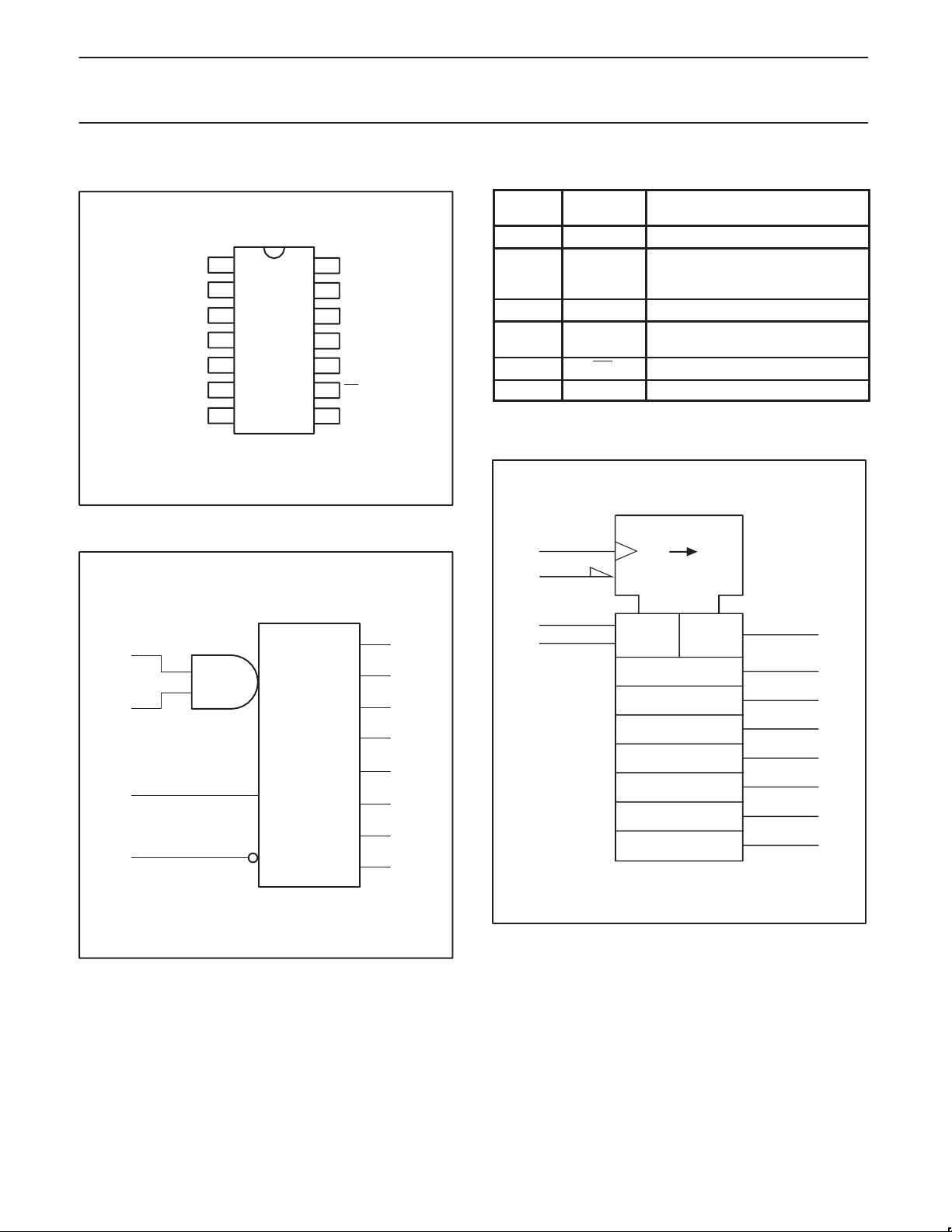
PIN CONFIGURATION
V
14
Q
13
Q
12
Q
11
Q
10
MR
9
CP
8
SV00381
CC
7
6
5
4
GND
LOGIC SYMBOL
D
1
sa
D
2
sb
Q
3
0
Q
4
1
Q
5
2
Q
6
3
7
PIN DESCRIPTION
PIN
NUMBER
1,2 Dsa, D
3, 4, 5, 6,
10, 11,
12, 13
7 GND Ground (0V)
8 CP
9 MR Master reset input (active LOW)
14 V
SYMBOL FUNCTION
Data inputs
sb
Q0 to Q7Outputs
Clock input (LOW-to-HIGH, edge-triggered)
CC
Positive supply voltage
LOGIC SYMBOL (IEEE/IEC)
SRG8
8
9
C1/
R
74LV164
1
Q
1
2
8
9
D
sa
D
sb
CP
MR
0
Q
1
Q
2
Q
3
Q
4
Q
5
Q
6
Q
7
3
4
5
6
10
11
12
13
SV00382
2
&
1D
3
4
5
6
10
11
12
13
SV00383
1998 May 07
3
Philips Semiconductors Product specification
8-bit serial-in/parallel-out shift register
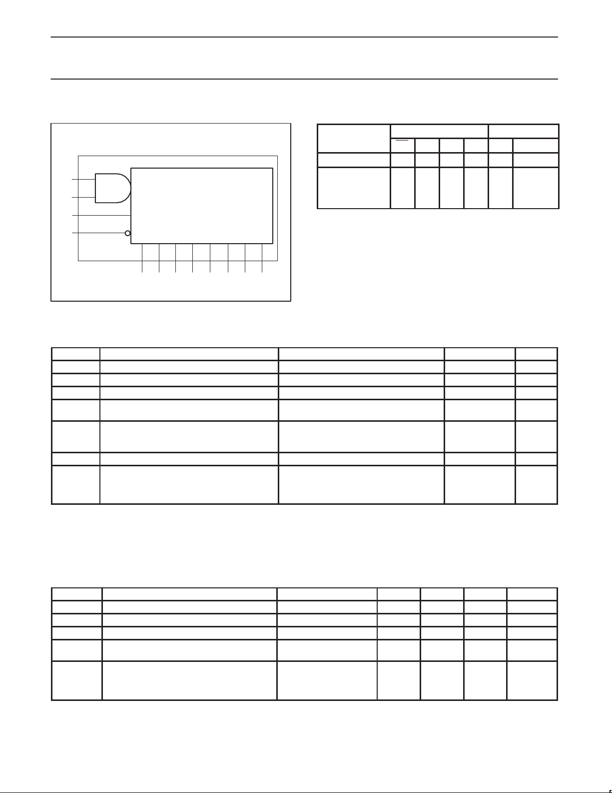
FUNCTIONAL DIAGRAM
D
sa
1
D
sb
2
CP
8
MR
9
ABSOLUTE MAXIMUM RATINGS
In accordance with the Absolute Maximum Rating System (IEC 134)
Voltages are referenced to GND (ground = 0V)
SYMBOL
V
CC
±I
±I
OK
±I
DC supply voltage –0.5 to +7.0 V
DC input diode current VI < –0.5 or VI > VCC + 0.5V 20 mA
IK
DC output diode current VO < –0.5 or VO > VCC + 0.5V 50 mA
DC output source or sink current
O
– standard outputs
8-BIT SERIAL-IN/PARALLEL-OUT
SHIFT REGISTER
Q
Q
0
3
1Q2Q3
5
4
Q
4Q5Q6Q7
6
10
11 12
13
SV00384
1, 2
PARAMETER CONDITIONS RATING UNIT
–0.5V < VO < VCC + 0.5V
74LV164
FUNCTION TABLE
OPERATING
MODES
Reset (clear) L X x x L L – L
Shift
H = HIGH voltage level
h = HIGH voltage level one set-up time prior to the
LOW-to-HIGH CP transition
L = LOW voltage level
l = LOW voltage level one set-up time prior to the
LOW-to-HIGH CP transition
q = Lower case letter indicates the state of referenced input
one set-up time prior to the LOW-to-HIGH CP transition
↑ = LOW-to-HIGH clock transition
INPUTS OUTPUTS
MR CP DsaD
H
↑
H
↑
H
↑
H
↑
sbQ0
l
l
l
h
h
l
h
h
25
Q1 – Q
L
q0 – q
q0 – q
L
q0 – q
L
q0 – q
H
mA
7
6
6
6
6
±I
GND
±I
CC
T
stg
P
TOT
DC VCC or GND current for types with
,
–standard outputs
50
Storage temperature range –65 to +150 °C
Power dissipation per package
–plastic DIL
–plastic mini-pack (SO)
–plastic shrink mini-pack (SSOP and TSSOP)
for temperature range: –40 to +125°C
above +70°C derate linearly with 12mW/K
above +70°C derate linearly with 8 mW/K
above +60°C derate linearly with 5.5 mW/K
750
500
400
mA
mW
NOTES:
1. Stresses beyond those listed may cause permanent damage to the device. These are stress ratings only and functional operation of the
device at these or any other conditions beyond those indicated under “recommended operating conditions” is not implied. Exposure to
absolute-maximum-rated conditions for extended periods may affect device reliability .
2. The input and output voltage ratings may be exceeded if the input and output current ratings are observed.
RECOMMENDED OPERATING CONDITIONS
SYMBOL PARAMETER CONDITIONS MIN TYP. MAX UNIT
V
CC
V
V
T
amb
tr, t
NOTES:
1. The LV is guaranteed to function down to V
DC supply voltage See Note 1 1.0 3.3 5.5 V
Input voltage 0 – V
I
Output voltage 0 – V
O
Operating ambient temperature range in free
air
Input rise and fall times
f
= 1.0V (input levels GND or VCC); DC characteristics are guaranteed from VCC = 1.2V to VCC = 5.5V.
CC
See DC and AC
characteristics
VCC = 1.0V to 2.0V
VCC = 2.0V to 2.7V
VCC = 2.7V to 3.6V
VCC = 3.6V to 5.5V
–40
–40
–
–
–
–
–
–
–
–
CC
CC
+85
+125
500
200
100
50
V
V
°C
ns/V
1998 May 07
4
 Loading...