

Philips 74LV154PW, 74LV154N, 74LV154DB, 74LV154D Datasheet

INTEGRATED CIRCUITS
74LV154
4-to-16 line decoder/demultiplexer
Product specification
Supersedes data of 1997 Mar 07
IC24 Data Handbook
1998 Apr 28

Philips Semiconductors Product specification
74L V1544-to-16 line decoder/demultiplexer
FEA TURES
•Optimized for low voltage applications: 1.0 to 3.6 V
•Accepts TTL input levels between V
•Typical V
T
amb
•Typical V
T
amb
(output ground bounce) < 0.8 V at V
OLP
= 25°C
(output VOH undershoot) > 2 V at V
OHV
= 25°C
= 2.7 V and V
CC
CC
CC
CC
= 3.3 V,
= 3.3 V,
•16-line demultiplexing capability
•Decodes 4 binary-coded inputs into one of 16 mutually
exclusive outputs
•2-input enable gate for strobing or expansion
•Output capability: standard
•I
category: MSI
CC
QUICK REFERENCE DATA
GND = 0 V; T
= 25°C; tr = t
amb
SYMBOL
t
PHL/tPLH
C
I
C
PD
NOTE:
1. C
is used to determine the dynamic power dissipation (PD in µW)
PD
= CPD × V
P
D
f
= input frequency in MHz; CL = output load capacitance in pF;
i
= output frequency in MHz; VCC = supply voltage in V;
f
o
× V
Σ (C
L
2
× fi +Σ (CL × V
CC
2
× fo) = sum of the outputs.
CC
≤ 2.5 ns
f
PARAMETER CONDITIONS TYPICAL UNIT
Propagation delay
An, En to Y
n
Input capacitance 3.5 pF
Power dissipation capacitance per gate VI = GND to V
2
× fo) where:
CC
= 3.6 V
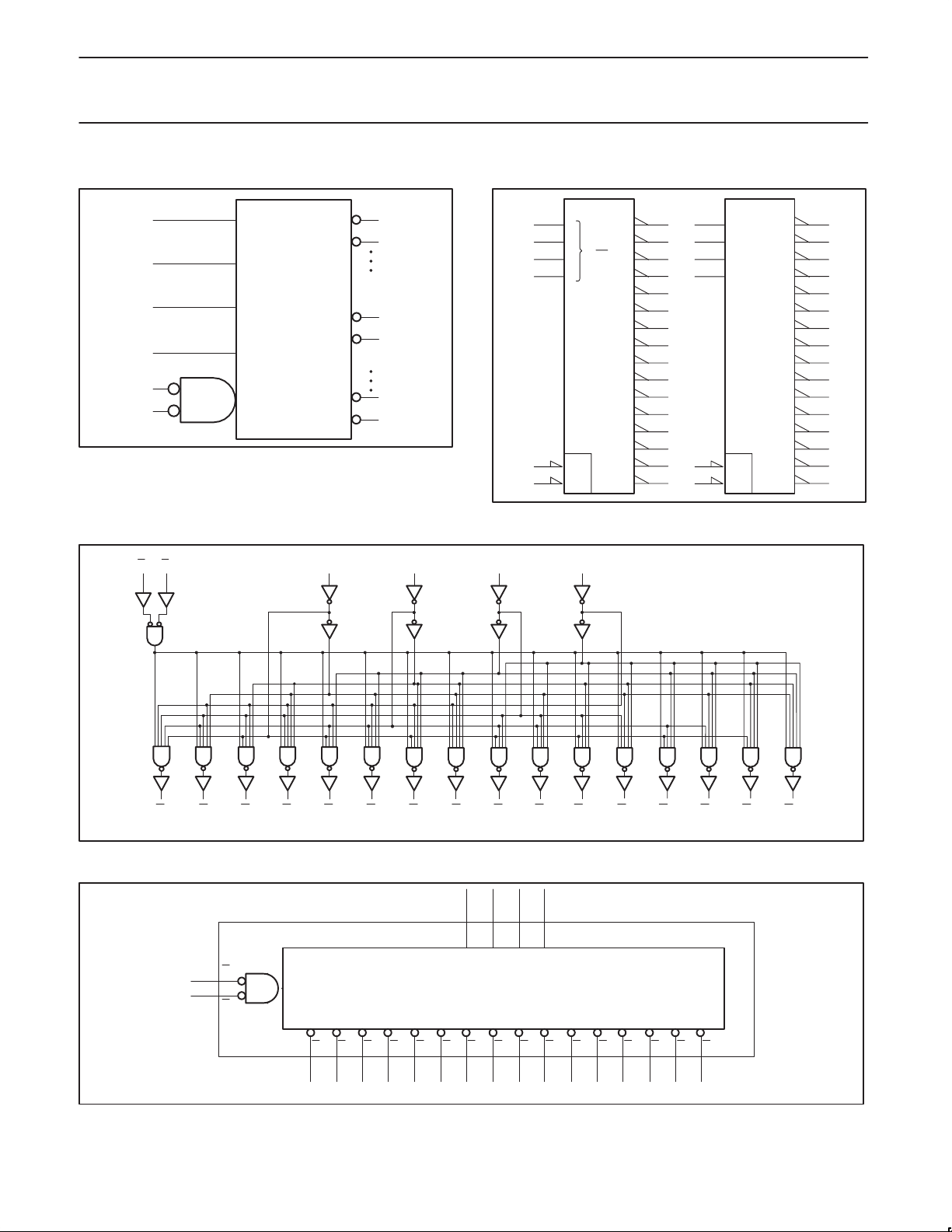
DESCRIPTION
The 74LV154 is a low-voltage CMOS device and is pin and function
compatible with 74HC/HCT154.
The 74LV154 decoders accept four active HIGH binary address
inputs (A
outputs(Y
The 2-input enable inputs (E0, E1) can be used to strobe the
decoder to eliminate the normal decoding “glitches” on the outputs,
or it can be used for expansion of the decoder.
The enable input has two AND’ed inputs which must be LOW to
enable the outputs.
The 74LV154 can be used as a 1-to-16 demultiplexer by using one
of the enable inputs as the multiplexed data input.
When the other enable is LOW, the addressed output will follow the
state of the applied data.
CL = 15 pF;
VCC = 3.3 V 11
to A3) and provide 16 mutually exclusive active LOW
0
to Y15).
0
CC
1
60 pF
ns
ORDERING INFORMATION
PACKAGES TEMPERATURE RANGE OUTSIDE NORTH AMERICA NORTH AMERICA PKG. DWG. #
24-Pin Plastic DIL –40°C to +125°C 74LV154 N 74LV154 N SOT101-1
24-Pin Plastic SO –40°C to +125°C 74LV154 D 74LV154 D SOT137-1
24-Pin Plastic SSOP Type II –40°C to +125°C 74LV154 DB 74LV154 DB SOT340-1
24-Pin Plastic TSSOP Type I –40°C to +125°C 74LV154 PW 74LV154PW DH SOT355-1
PIN CONFIGURATION
Y
1
0
Y
2
1
3
Y
2
Y
4
3
5
Y
4
Y
6
5
Y
7
6
Y
8
7
9
Y
8
10
Y
9
Y
11
10
GND
12
V
24
CC
23
A
0
A
22
1
A
21
2
A
20
3
19
E
1
E
18
0
Y
17
15
Y
16
14
Y
15
13
Y
14
12
Y
13
11
SV00544
PIN DESCRIPTION
PIN NUMBER SYMBOL FUNCTION
1, 2, 3, 4, 5, 6, 7,
8, 9, 10, 11, 13,
14, 15, 16, 17
18, 19 E0, E
12 GND Ground (0 V)
23, 22, 21, 20 A0 to A
16 V
Y0 to Y
CC
Outputs (active LOW)
15
Enable inputs (active LOW)
1
Address inputs
3
Positive supply voltage
1998 Apr 28 853–1939 19309
2
Philips Semiconductors Product specification
4-to-16 line decoder/demultiplexer
LOGIC SYMBOL
23
22
21
20
E
18
19
0
E
1
LOGIC DIAGRAM
A
0
A
1
A
2
A
3
Y
0
Y
1
Y
10
Y
11
Y
14
Y
15
SV00545
74LV154
LOGIC SYMBOL (IEEE/IEC)
1
2
11
13
16
17
23 23
22 22
21 21
20 20
18
19
DX X/Y
01
0
G
15
38
&
11
00
22
11
33
22
44
33
55
44
66
55
77
66
88
77
99
88
10 10
99
11 11
10 10
13 13
11 11
14 14
12 12
15 15
13 13
16 16
14 14
17 17
15 15
2
4
&
18
19
EN
SV00546
E1E
0
Y
Y
0
Y
1
FUNCTIONAL DIAGRAM
18
E
0
19
E
1
A
0
Y
2
Y
3
4
A
1
Y
Y
6
5
Y
7
DECODER
A
2
Y
8
23
A
21
22
A
A
0
1
A
3
Y
Y
9
10
20
A
3
2
Y
Y
Y
12
11
Y
14
Y
SV00548
15
13
1998 Apr 28
Y
Y
0
1
2
Y
Y
Y
Y
Y
Y
Y
Y
Y
Y
Y
Y
Y
3
4
5
6
7
8
9
10
11
2
1
4
5
6
7
8
9
10
3
11
12
13
14
15
Y
13
14
15
16
17
SV00547
3
Philips Semiconductors Product specification
4-to-16 line decoder/demultiplexer
74LV154
FUNCTION TABLE
INPUTS OUTPUTS
E0E1A0A1A2A3Y0Y1Y2Y3Y4Y5Y6Y7Y8Y9Y10Y11Y12Y13Y14Y
H H X X X X H H H H H H H H H H H H H H H H
H L X X X X H H H H H H H H H H H H H H H H
L H X X X X H H H H H H H H H H H H H H H H
L L L L L L L H H H H H H H H H H H H H H H
L L H L L L H L H H H H H H H H H H H H H H
L L L H L L H H L H H H H H H H H H H H H H
L L H H L L H H H L H H H H H H H H H H H H
L L L L H L H H H H L H H H H H H H H H H H
L L H L H L H H H H H L H H H H H H H H H H
L L L H H L H H H H H H L H H H H H H H H H
L L H H H L H H H H H H H L H H H H H H H H
L L L L L H H H H H H H H H L H H H H H H H
L L H L L H H H H H H H H H H L H H H H H H
L L L H L H H H H H H H H H H H L H H H H H
L L H H L H H H H H H H H H H H H L H H H H
L L L L H H H H H H H H H H H H H H L H H H
L L H L H H H H H H H H H H H H H H H L H H
L L L H H H H H H H H H H H H H H H H H L H
L L H H H H H H H H H H H H H H H H H H H L
NOTES:
H = HIGH voltage level
L = LOW voltage level
X = don’t care
15
RECOMMENDED OPERATING CONDITIONS
SYMBOL PARAMETER CONDITIONS MIN TYP MAX UNIT
V
V
V
T
amb
tr, t
NOTE:
1. The LV is guaranteed to function down to V
DC supply voltage See Note 1 1.0 3.3 3.6 V
CC
Input voltage 0 – V
I
Output voltage 0 – V
O
Operating ambient temperature range in free air
Input rise and fall times
f
CC
See DC and AC
characteristics
VCC = 1.0V to 2.0V
VCC = 2.0V to 2.7V
V
= 2.7V to 3.6V
CC
= 1.0V (input levels GND or VCC); DC characteristics are guaranteed from VCC = 1.2V to VCC = 3.6V.
–40
–40
–
–
–
–
–
–
CC
CC
+85
+125
500
200
100
ns/V
V
V
°C
1998 Apr 28
4
 Loading...