

Philips 74LV14D, 74LV14U, 74LV14PW, 74LV14N, 74LV14DB Datasheet
74LV14
Hex inverting Schmitt-trigger
Product specification
Supersedes data of 1997 Feb 03
IC24 Data Handbook
1998 Apr 20
INTEGRATED CIRCUITS
Philips Semiconductors Product specification
74L V14Hex inverting Schmitt-trigger
2
1998 Apr 20 853–1895 19256
FEA TURES
•Wide operating voltage: 1.0 to 5.5 V
•Optimized for Low Voltage applications: 1.0 to 3.6 V
•Accepts TTL input levels between V
CC
= 2.7 V and VCC = 3.6 V
•Typical V
OLP
(output ground bounce) < 0.8 V at VCC = 3.3 V,
T
amb
= 25°C.
•Typical V
OHV
(output VOH undershoot) > 2 V at VCC = 3.3 V,
T
amb
= 25°C.
•Output capability: standard
•I
CC
category: SSI
APPLICATIONS
•Wave and pulse shapers for highly noisy environments
DESCRIPTION
The 74LV14 is a low-voltage Si-gate CMOS device and is pin and
function compatible with 74HC/HCT14.
The 74LV14 provides six inverting buffers with Schmitt-trigger
action. It is capable of transforming slowly changing input signals
into sharply defined, jitter-free output signals.
QUICK REFERENCE DA TA
GND = 0 V; T
amb
= 25°C; tr = tf ≤ 2.5 ns
SYMBOL
PARAMETER CONDITIONS TYPICAL UNIT
t
PHL/tPLH
Propagation delay
nA to nY
CL = 15 pF;
VCC = 3.3 V
13 ns
C
I
Input capacitance 3.5 pF
C
PD
Power dissipation capacitance per gate See Notes 1 and 2 15 pF
NOTES:
1. C
PD
is used to determine the dynamic power dissipation (PD in µW)
P
D
= CPD × V
CC
2
× fi (CL × V
CC
2
× fo) where:
f
i
= input frequency in MHz; CL = output load capacitance in pF;
f
o
= output frequency in MHz; VCC = supply voltage in V;
(C
L
× V
CC
2
× fo) = sum of the outputs.
2. The condition is V
I
= GND to V
CC.
ORDERING INFORMATION
PACKAGES TEMPERATURE RANGE OUTSIDE NORTH AMERICA NORTH AMERICA PKG. DWG. #
14-Pin Plastic DIL –40°C to +125°C 74LV14 N 74LV14 N SOT27-1
14-Pin Plastic SO –40°C to +125°C 74LV14 D 74LV14 D SOT108-1
14-Pin Plastic SSOP Type II –40°C to +125°C 74LV14 DB 74LV14 DB SOT337-1
14-Pin Plastic TSSOP Type I –40°C to +125°C 74LV14 PW 74LV14PW DH SOT402-1
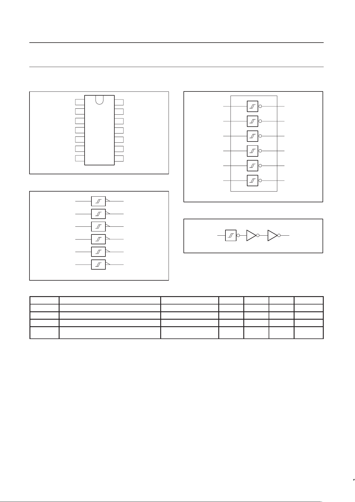
PIN DESCRIPTION
PIN NUMBER SYMBOL NAME AND FUNCTION
1, 3, 5, 9, 11, 13 1A – 6A Data inputs
2, 4, 6, 8, 10, 12 1Y – 6Y Data outputs
7 GND Ground (0 V)
14 V
CC
Positive supply voltage
FUNCTION TABLE
INPUT OUTPUT
nA nY
L H
H L
NOTES:
H = HIGH voltage level
L = LOW voltage level
Philips Semiconductors Product specification
74LV14Hex inverting Schmitt-trigger
1998 Apr 20
3
PIN CONFIGURATION
1
2
3
4
5
6
7
1A
1Y
2A
2Y
3A
3Y
GND
V
CC
6A
6Y
5A
5Y
4A
4Y
14
13
12
11
10
9
8
SV00396
LOGIC SYMBOL (IEEE/IEC)
SV00425
1
2
3
4
5
6
9
8
11
10
13
12
LOGIC SYMBOL
SV00424
1A 1Y
2A
2Y
3A 3Y
4A 4Y
5A 5Y
6A
6Y
1
3
5
9
11
13
2
4
6
8
10
12
LOGIC DIAGRAM
SV00426
AY
RECOMMENDED OPERA TING CONDITIONS
SYMBOL PARAMETER CONDITIONS MIN TYP MAX UNIT
V
CC
DC supply voltage See Note1 1.0 3.3 5.5 V
V
I
Input voltage 0 – V
CC
V
V
O
Output voltage 0 – V
CC
V
T
amb
Operating ambient temperature range in free
air
See DC and AC
characteristics
–40
–40
+85
+125
°C
NOTE:
1. The LV is guaranteed to function down to V
CC
= 1.0V (input levels GND or VCC); DC characteristics are guaranteed from VCC = 1.2V to VCC = 5.5V.

Philips Semiconductors Product specification
74LV14Hex inverting Schmitt-trigger
1998 Apr 20
4
ABSOLUTE MAXIMUM RATINGS
1, 2
In accordance with the Absolute Maximum Rating System (IEC 134).
Voltages are referenced to GND (ground = 0V).
SYMBOL
PARAMETER CONDITIONS RATING UNIT
V
CC
DC supply voltage –0.5 to +7.0 V
I
IK
DC input diode current VI < –0.5 or VI > VCC + 0.5V 20 mA
I
OK
DC output diode current VO < –0.5 or VO > VCC + 0.5V 50 mA
I
O
DC output source or sink current
– standard outputs
–0.5V < VO < VCC + 0.5V
25
mA
I
GND
,
I
CC
DC VCC or GND current for types with
– standard outputs 50
mA
T
stg
Storage temperature range –65 to +150 °C
P
TOT
Power dissipation per package
– plastic DIL
– plastic mini-pack (SO)
– plastic shrink mini-pack (SSOP and TSSOP)
for temperature range: –40 to +125°C
above +70°C derate linearly with 12 mW/K
above +70°C derate linearly with 8 mW/K
above +60°C derate linearly with 5.5 mW/K
750
500
400
mW
NOTES:
1. Stresses beyond those listed may cause permanent damage to the device. These are stress ratings only and functional operation of the
device at these or any other conditions beyond those indicated under “recommended operating conditions” is not implied. Exposure to
absolute-maximum-rated conditions for extended periods may affect device reliability .
2. The input and output voltage ratings may be exceeded if the input and output current ratings are observed.
DC ELECTRICAL CHARACTERISTICS
Over recommended operating conditions. V oltages are referenced to GND (ground = 0V).
LIMITS
SYMBOL P ARAMETER TEST CONDITIONS
-40°C to +85°C -40°C to +125°C
UNIT
MIN TYP
1
MAX MIN MAX
VCC = 1.2V; VI = VIH or V
IL;
–IO = 100µA 1.2
VCC = 2.0V; VI = VIH or V
IL;
–IO = 100µA 1.8 2.0 1.8
V
OH
HIGH l
evel outpu
t
;
p
VCC = 2.7V; VI = VIH or V
IL;
–IO = 100µA 2.5 2.7 2.5
V
voltage all out uts
VCC = 3.0V; VI = VIH or V
IL;
–IO = 100µA 2.8 3.0 2.8
VCC = 4.5V; VI = VIH or V
IL;
–IO = 100µA 4.3 4.5 4.3
HIGH level output
voltage;
VCC = 3.0V; VI = VIH or V
IL;
–IO = 6mA 2.40 2.82 2.20
V
OH
g
STANDARD
outputs
VCC = 4.5V; VI = VIH or V
IL;
–IO = 12mA 3.60 4.20 3.50
V
VCC = 1.2V; VI = VIH or V
IL;
IO = 100µA 0
VCC = 2.0V; VI = VIH or V
IL;
IO = 100µA 0 0.2 0.2
V
OL
LOW l
evel outpu
t
;
p
VCC = 2.7V; VI = VIH or V
IL;
IO = 100µA 0 0.2 0.2
V
voltage all out uts
VCC = 3.0V; VI = VIH or V
IL;
IO = 100µA 0 0.2 0.2
VCC = 4.5V; VI = VIH or V
IL;
IO = 100µA 0 0.2 0.2
LOW level output
voltage;
VCC = 3.0V; VI = VIH or V
IL;
IO = 6mA 0.25 0.40 0.50
V
OL
g
STANDARD
outputs
VCC = 4.5V; VI = VIH or V
IL;
IO = 12mA 0.35 0.55 0.65
V
I
I
Input leakage
current
VCC = 5.5V; VI = VCC or GND 1.0 1.0 µA
I
CC
Quiescent supply
current; SSI
VCC = 5.5V; VI = VCC or GND; IO = 0 20.0 40 µA
∆I
CC
Additional
quiescent supply
current
VCC = 2.7V to 3.6V; VI = VCC – 0.6V 500 850 µA
NOTE:
1. All typical values are measured at T
amb
= 25°C.
 Loading...