

Philips 74LV138PW, 74LV138N, 74LV138DB, 74LV138D Datasheet

INTEGRATED CIRCUITS
74LV138
3-to-8 line decoder/multiplexer; inverting
Product specification
Supersedes data of 1997 Feb 03
IC24 Data Handbook
1998 Apr 28
Philips Semiconductors Product specification
74L V1383-to-8 line decoder/demultiplexer; inverting
FEA TURES
•Wide operating voltage: 1.0 to 5.5 V
•Optimized for low voltage applications: 1.0 to 3.6 V
•Accepts TTL input levels between V
•Typical V
T
amb
•Typical V
T
amb
(output ground bounce) < 0.8 V at V
OLP
= 25°C
(output VOH undershoot) > 2 V at V
OHV
= 25°C
= 2.7 V and V
CC
CC
CC
CC
= 3.3 V,
= 3.3 V,
•Demultiplexing capability
•Multiple input enable for easy expansion
•Ideal for memory chip select decoding
•Active LOW mutually exclusive outputs
•Output capability: standard
•I
category: MSI
CC
QUICK REFERENCE DATA
GND = 0 V; T
= 25°C; tr = t
amb
SYMBOL
t
PHL/tPLH
C
I
C
PD
NOTES:
is used to determine the dynamic power dissipation (PD in µW)
1. C
PD
P
= CPD × V
D
= input frequency in MHz; CL = output load capacitance in pF;
f
i
f
= output frequency in MHz; VCC = supply voltage in V;
o
× V
(C
L
2
× fi (CL × V
CC
2
× fo) = sum of the outputs.
CC
≤ 2.5 ns
f
PARAMETER CONDITIONS TYPICAL UNIT
Propagation delay
An to Yn,
E3 to Yn, En to Yn
Input capacitance 3.5 pF
Power dissipation capacitance per
package
2
× fo) where:
CC
= 3.6 V
DESCRIPTION
The 74LV138 is a low-voltage Si-gate CMOS device that is pin and
function compatible with 74HC/HCT138.
The 74LV138 accepts three binary weighted address inputs (A
A
) and when enabled, provide 8 mutually exclusive active LOW
2
outputs (Y
The 74LV138 features three enable inputs: two active LOW (E1, and
E
) and one active HIGH (E3). Every output will be HIGH unless E
2
and E2 are LOW and E3 is HIGH.
This multiple enable function allows easy parallel expansion of the
74LV138 to a 1-of-32 (5 lines to 32 lines) decoder with just four
74LV138 ICs and one inverter. The 74LV138 can be used as an
eight output demultiplexer by using one of the active LOW enable
inputs as the data input and the remaining enable inputs as strobes.
Unused enable inputs must be permanently tied to their appropriate
active HIGH or LOW state. The 74LV138 is identical to the 74LV238
but has non-inverting (true) outputs.
CL = 15 pF;
VCC = 3.3 V
VCC = 3.3 V
V
= GND to V
I
CC
to Y7).
0
1
12
14
45 pF
ns
ns
, A1,
0
1
ORDERING INFORMATION
PACKAGES TEMPERATURE RANGE OUTSIDE NORTH AMERICA NORTH AMERICA PKG. DWG. #
16-Pin Plastic DIL –40°C to +125°C 74LV138 N 74LV138 N SOT38-4
16-Pin Plastic SO –40°C to +125°C 74LV138 D 74LV138 D SOT109-1
16-Pin Plastic SSOP Type II –40°C to +125°C 74LV138 DB 74LV138 DB SOT338-1
16-Pin Plastic TSSOP Type I –40°C to +125°C 74LV138 PW 74LV138PW DH SOT403-1
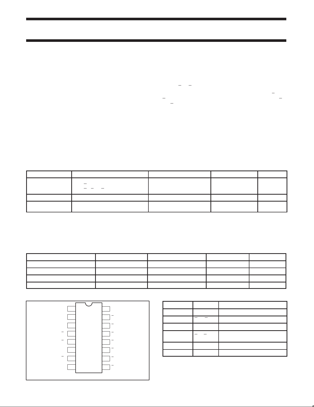
PIN CONFIGURATION
1
A
0
2
A
1
3
A
2
4
E
1
5
E
2
6
E
3
Y
7
7
GND
8
1998 Apr 28 853–1903 19290
16
15
14
13
12
11
10
9
SV00524
V
CC
Y
0
Y
1
Y
2
Y
3
Y
4
Y
5
Y
6
PIN DESCRIPTION
PIN NUMBER SYMBOL FUNCTION
1, 2, 3 A0 to A
4, 5 E1 to E
6 E
15, 14, 13, 12,
11, 10, 9, 7
3
Y
Y
0 to
8 GND Ground (0 V)
16 V
CC
2
Address inputs
2
Enable inputs (active LOW)
2
Enable inputs (active HIGH)
Outputs
7
Positive supply voltage
Philips Semiconductors Product specification
3-to-8 line decoder/demultiplexer; inverting
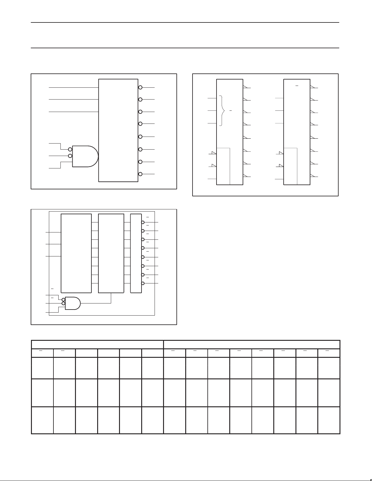
LOGIC DIAGRAM
1
2
3
4
E
1
5
6
E
2
E
3
FUNCTIONAL DIAGRAM
A
0
A
1
A
2
Y
0
Y
1
Y
2
Y
3
Y
4
Y
5
Y
6
Y
7
15
14
13
12
11
10
9
7
SV00525
LOGIC SYMBOL (IEEE/IEC)
DX
0
15
1
0
2
23
4
5
6
1
14
0
G
7
&
(a)
13
2
12
3
11
4
10
5
6
9
7
7
74LV138
X
0
1
2
3
4
5
6
7
SV00526
15
14
13
12
11
10
9
7
Y
1
1
2
2
4
3
4
5
6
&
EN
(b)
Y
0
15
Y
A
0
1
A
1
2
A
3
E
4
E
5
E
6
3-to-8
2
DECODER
1
2
3
ENABLE
EXITING
1
Y
2
Y
3
Y
4
Y
5
Y
6
Y
7
SV00527
14
13
12
11
10
9
7
FUNCTION TABLE
INPUTS OUTPUTS
E
1
H X X X X X H H H H H H H H
X H X X X X H H H H H H H H
X X L X X X H H H H H H H H
L L H L L L L H H H H H H H
L L H H L L H L H H H H H H
L L H L H L H H L H H H H H
L L H H H L H H H L H H H H
L L H L L H H H H H L H H H
L L H H L H H H H H H L H H
L L H L H H H H H H H H L H
L L H H H H H H H H H H H L
NOTES:
H = HIGH voltage level
L = LOW voltage level
X = don’t care
E
2
E
3
A
A
0
1
A
2
Y
0
Y
1
Y
2
Y
3
Y
4
Y
5
Y
6
Y
7
1998 Apr 28
3

Philips Semiconductors Product specification
3-to-8 line decoder/demultiplexer; inverting
74LV138
RECOMMENDED OPERATING CONDITIONS
SYMBOL PARAMETER CONDITIONS MIN TYP MAX UNIT
V
V
V
T
amb
tr, t
NOTE:
1. The LV is guaranteed to function down to V
ABSOLUTE MAXIMUM RATINGS
In accordance with the Absolute Maximum Rating System (IEC 134).
Voltages are referenced to GND (ground = 0 V).
SYMBOL
V
I
I
I
DC supply voltage See Note 1 1.0 3.3 5.5 V
CC
Input voltage 0 – V
I
Output voltage 0 – V
O
Operating ambient temperature range in free air
Input rise and fall times
f
CC
See DC and AC
characteristics
VCC = 1.0V to 2.0V
VCC = 2.0V to 2.7V
VCC = 2.7V to 3.6V
VCC = 3.6V to 5.5V
= 1.0V (input levels GND or VCC); DC characteristics are guaranteed from VCC = 1.2V to VCC = 5.5V.
–40
–40
–
–
–
–
–
–
–
–
1, 2
PARAMETER CONDITIONS RATING UNIT
CC
DC supply voltage –0.5 to +7.0 V
DC input diode current VI < –0.5 or VI > VCC + 0.5V 20 mA
IK
DC output diode current VO < –0.5 or VO > VCC + 0.5V 50 mA
OK
DC output source or sink current
O
– standard outputs
–0.5V < VO < VCC + 0.5V
25
CC
CC
+85
+125
500
200
100
50
ns/V
V
V
°C
mA
I
I
P
GND
T
TOT
stg
DC VCC or GND current for types with
,
– standard outputs 50
CC
Storage temperature range –65 to +150 °C
Power dissipation per package
– plastic DIL
– plastic mini-pack (SO)
– plastic shrink mini-pack (SSOP and TSSOP)
for temperature range: –40 to +125°C
above +70°C derate linearly with 12 mW/K
above +70°C derate linearly with 8 mW/K
above +60°C derate linearly with 5.5 mW/K
750
500
400
mA
mW
NOTES:
1. Stresses beyond those listed may cause permanent damage to the device. These are stress ratings only and functional operation of the
device at these or any other conditions beyond those indicated under “recommended operating conditions” is not implied. Exposure to
absolute-maximum-rated conditions for extended periods may affect device reliability .
2. The input and output voltage ratings may be exceeded if the input and output current ratings are observed.
1998 Apr 28
4
 Loading...