


INTEGRATED CIRCUITS
DATA SH EET
For a complete data sheet, please also download:
•The IC06 74HC/HCT/HCU/HCMOS Logic Family Specifications
•The IC06 74HC/HCT/HCU/HCMOS Logic Package Information
•The IC06 74HC/HCT/HCU/HCMOS Logic Package Outlines
74HC/HCT7132
Quad precision adjustable
Schmitt-trigger / comparator with
output latches; 3-state
Product specification
File under Integrated Circuits, IC06
September 1993

Philips Semiconductors Product specification
Quad precision adjustable Schmitt-trigger /
comparator with output latches; 3-state
FEATURES
• Precision inputs
• 2 operation modes: PAST and
comparator
• In PAST mode: Inverting outputs in
view of the precision oscillator
application
• In comparator mode: Non-inverting
outputs to simplify the design of an
external hysteresis network
• 3-state outputs for bus oriented
applications
• Output capability: Bus driver
• ICC category: MSI
APPLICATIONS
• Precision oscillators
• Signal reconditioning
• Level conversion
• Process control (temperature,
pressure, power e.g.)
• Accurate level detectors
• Time delays
• Overvoltage, overcurrent
protection
• Bargraph display with LED’s
• Battery charge control
• Analog to digital conversion
DESCRIPTION
The 74HC/HCT7132 are high-speed
Si-gate CMOS devices. They are
specified in compliance with JEDEC
standard no. 7A.
The 74HC/HCT7132 contain 4
comparators with two common
74HC/HCT7132
reference inputs V
separate signal inputs V
The circuits can be applied in two
modes:
1. The PAST (precision adjustable
Schmitt-trigger) mode at which a
voltage level equal to the wanted
VT+must be applied to the
VrHinput and a voltage level
equal to the wanted VT−to the
VrLinput.
2. The comparator mode at which
the VrLinput must be connected
to GND and the VrHinput is the
active reference level input. In
this mode a few resistors must be
added to achieve a small
hysteresis in order to avoid
oscillations. The operation in both
modes will be further explained
by means of the logic diagram of
Fig.5.
and VrLand four
rH
to V
in0
in3
.
QUICK REFERENCE DATA
GND = 0 V; T
= 25 °C; tr= tf= 6 ns
amb
SYMBOL PARAMETER CONDITIONS TYPICAL UNIT
V
V
δV
C
rH
rL
t
PD
High trip level PAST mode; VCC= 3 to 6 V 1.15 to VCC− 1.2 V
reference level Comparator mode; V
= 3 to 6 V 0.6 to V
CC
CC
V
Low trip level PAST mode; VCC= 3 to 6 V 1.10 to VCC− 1.25 V
DC inaccuracy VCC= 3 to 6 V ±20 mV
power dissipation
capacitance per function
VCC=5 V
PAST mode 100 pF
Comparator mode 30 pF
P
d
t
rmin/tfmin
t
PHL/tPLH
Total DC power dissipation Comparator mode; VCC= 4.5 V;
Minimum rise and fall time
for optimum operation
propagation delay
V
to Q
inn
VrL=V
PAST mode; VCC= 4.5 V;
VrH= 3 V; VrL= 1.5 V
PAST mode; VCC= 4.5 V 40/60 ns
= 0 V; VrH= 2.25 V
INn
8mW
180 ns
Notes
1. C
is used to determine the dynamic power dissipation (PDin µW):
PD
PD= CPD× V
2
× fi+ CL× V
CC
2
× fowhere:
CC
fi= input frequency in MHz;
fo= output frequency in MHz;
CL= output load capacity in pF;
VCC= supply voltage in V.
September 1993 2
Philips Semiconductors Product specification
Quad precision adjustable Schmitt-trigger /
74HC/HCT7132
comparator with output latches; 3-state
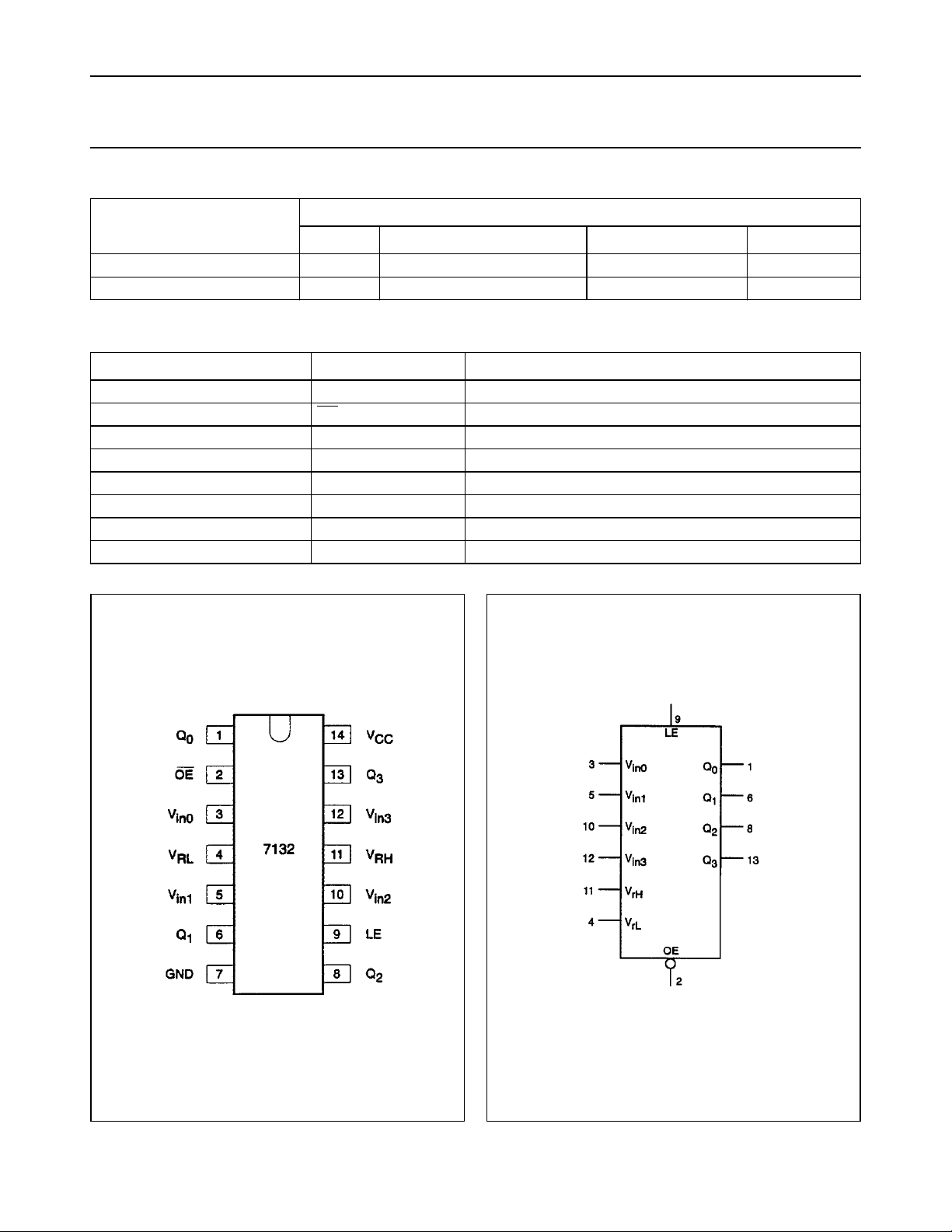
ORDERING INFORMATION
TYPE NUMBER
PINS PIN POSITION MATERIAL CODE
74HC/HCT7132P 14 DIL plastic SOT27
74HC/HCT7132T 14 SO plastic SOT108
PINNING
PIN SYMBOL NAME AND FUNCTION
1, 6, 8, 13 Q
2
3, 5, 10, 12 V
4V
to Q
0
3
OE 3-state output enable input (active LOW)
to V
in0
in3
rL
3-state latch outputs
signal inputs
low reference voltage input
7 GND ground (0 V)
9 LE latch enable input (active HIGH)
11 V
14 V
rH
CC
high reference voltage input
positive supply voltage
PACKAGE
Fig.1 Pin configuration. Fig.2 Logic symbol.
September 1993 3
Philips Semiconductors Product specification
Quad precision adjustable Schmitt-trigger /
comparator with output latches; 3-state
Table 1 Function table for PAST mode
(rising edge) LE OE Q
V
inn
V
< V
inn
LL
V
< V
LL
V
HH
V
inn
VHH> V
V
LL
V
inn
V
inn
V
inn
< V
inn
rH
> V
> V
inn
rH
> V
HH
V
(falling edge) LE OE Q
inn
> V
inn
rL
< V
< V
inn
rL
< V
LL
=X H L Q
=X X H Z
LLH
LLH
LLL
LLL
LLL
LLH
LLH
Note
1. H = HIGH voltage level
L = LOW voltage level
Z = high impedance OFF-state
X = don’t care
= initial state
Q
t−1
DETAILED DESCRIPTION
The mode selector.
See Fig.5 for logic diagram. The circuit can be applied in
two modes that are selected by the mode selector on
bases of the level on the V
input. When the level on this
rL
input is in the operating area of the PAST mode (VrL> 1 V)
the true output of the mode detector is “0“ which means
that the PAST mode is selected. When the VrLinput is at
GND level the true output of the mode detector is “1” by
which the comparator mode is selected. This mode needs
only one reference input being the VrHinput.
The Power-on Detector
The power-on detector selects a window typically between
V
= 1 V and V
INn
INn=VCC
− 1 V in which in case of the
PAST mode the power of the analog part (comparator) is
switched on. When operating in the comparator mode the
power is always switched on by means of an OR gate.
The digital detector
The digital detector is a Flip-Flop which output is set to
LOW when V
V
> VCC− 1 V. This detector controls the output stage in
INn
< 1 V and to HIGH when
INn
the cases that the power of the comparator is switched off.
This is performed by means of the switches SW3and SW4.
n
n
t-1
74HC/HCT7132
The latch
The output information can be stored in a latch on
activating the LE input. In the PAST mode this latch is also
used to control the reference input of the comparator which
is either connected to the VrHinput via SW1or to the
VrLinput via SW2. In case of the comparator mode the
reference input is always connected to the VrHinput. This
is done by means of an AND gate.
The exclusive OR gate
By means of this function the output stage is switched
between inverting and non-inverting. In the PAST mode
the inverting output of the mode selector is “1” so the
exclusive OR is inverting. In the comparator mode this
output is “0” so the exclusive OR is non-inverting.
The operation in the PAST mode
The operation in the PAST mode will be further outlined
with the aid of Fig.5 and 9. and Table 1. When the level of
V
is 0 V the power of the comparator is switched OFF
INn
and the output circuit is controlled by the digital detector
which output is LOW in that situation. So the output of the
transparent latch is LOW. As the output stage is inverting
now Qnis HIGH. In this condition the reference input of the
comparator is connected to the +VrHinput. When starting
from 0 V the level at V
VLLlevel (≈1 V) the DC power of the comparator is
switched ON. The control of the output circuit is switched
over from the digital detector output to the comparator
output, when after a delay the voltage at this node is
stabilised. During this operation the output level of the
latch output remains LOW and the level of QnHIGH. When
the level at V
reaches the VrHlevel the output level of the
inn
comparator turns to HIGH and so the output level of the
transparent latch. The level at Qnturns to LOW. In this
instant the reference input of the comparator is switched
over from VrHto VrLleaving the output voltage at
Qnconstant. When the level at V
(≈ VCC− 1 V) the DC power of the comparator is switched
OFF. The control of the output circuit is switched over from
the comparator output to the digital detector output which
voltage level is HIGH in this situation. During this action the
level at Qnremains LOW. When the level at the V
is decreased starting at VCClevel, at the VHHlevel
(≈VCC− 1 V) the power of the comparator will be switched
on again. The control of the output circuit is switched over
from the digital detector output to the comparator output
when after a delay the voltage at this node is stabilised. As
the comparator output level is HIGH in this situation the
output level of the latch remains HIGH and the Qn output
LOW. When the level at V
is increased, at about the
inn
reaches the VHHlevel
inn
reaches the VrLlevel the
inn
inn
input
September 1993 4

Philips Semiconductors Product specification
Quad precision adjustable Schmitt-trigger /
comparator with output latches; 3-state
output level of the comparator turns to LOW and so the
output level of the transparent latch. The level at Qnturns
to HIGH. In this instant the reference input of the
comparator is switched over from VrLto VrHleaving the
output voltage at Qnconstant. When the level at
V
reaches about 1 V the DC power of the comparator is
inn
switched OFF again. The control of the output circuit is
switched over from the comparator output to the digital
detector output which voltage level is LOW in this situation.
During this action the level at Qnremains HIGH. The
function of the circuit is a Schmitt-trigger of which the
VT+and VT−levels can be set at the VrHand VrLinputs.
These levels can be varied from ≈1 V up to ≈VCC− 1 V. so
the maximum obtainable hysteresis is ≈VCC− 2 V. The
on-and off switching of the power and the stabilization of
the comparator needs time, therefore the minimum
applicable rise- and fall time of the input signal are limited
when the maximum accuracy is required. When during the
rise time of the input signal the input level has past the
VLLlevel, the power starts to switch on. Only when the
comparator is stable at the moment that the input signal
passes the VrHlevel the comparator has its true delay and
its optimal accuracy. When the VrHlevel is passed before
the comparator is stable an extra delay occurs due to the
switching of the power and the accuracy of the comparator
is less. At the positive going edge, this extra delay
depends on the difference between VLLand VrHand the
rise time of the signal. This is shown in Fig.8, where by
means of curves A and B t
and 2.25 V respectively and VCC= 4.5 V. As with curve a
VrHis very close to VLLthe part of the input edge that is
available for switching the power on is very small. This
causes that only at a rise time > 500 ns/V the delay will be
equal to the true delay of the comparator. At VrH= 2.25 V
this situation is reached already at a rise time of 120 ns/V.
At a very short rise time, the major part of the propagation
delay is due to the switching time of the power. At the
negative going edge, the power is switched on when the
level VHHis passed so the extra delay depends on the
difference between VHHand VrL and the fall time of the
signal. This situation is referred to with curves C and D
where t
is drawn against the fall time of the input signal.
PLH
With curve C VrLis 3.25 V which is on the edge of the
operating region. Curve D corresponds with a VrLvalue of
2.25 V. For linear input edges the recommended minimum
rise time at VCC= 4.5 V or 6 V is 100 ns/V and at
VCC= 3 V, 300 ns/V. For non-linear input signals, during
the rising edge there must be a delay between the time at
which the VLLlevel is passed and the time at which the
VrHlevel is passed. This delay will be dependent on the
VCClevel and the amplitude of the overdrive of VLL. There
is no limitation on the signal slope during the passing of the
levels. For the same reasons, during the falling edge there
is plotted at VrHis 1.15 V
PHL
74HC/HCT7132
must be a delay between the time at which the VHHlevel is
passed and the time at which the VrLlevel is passed.
A possible application of the circuit is as precision
oscillator see Fig.6. The operating frequency is:
=
f
-----------------------------------------------------------t
RC
where t
RC
The operation in the comparator mode
The IC can be applied as a comparator by connecting the
input to GND and adjusting the level at VrHto the
V
rL
wanted detection level see Fig.7. In this mode the DC
power of the comparator is always on and the output stage
is set to non-inverting. The function table for this operation
mode is given in table 2.
Table 2 Function table for Comparator mode
INPUT LE OE Q
V
< V
inn
ref
V
inn>Vref
V
=X H L Q
inn
V
=X X H Z
inn
Notes
1. H = HIGH voltage level
L = LOW voltage level
Z = high impedance OFF-state
X = don’t care
The fact that the power is always on offers the feature of a
more extended operation region of the V
which is at a VCCof 4.5 V from 1.1 V up to 4.2 V see also
Fig.12. A hysteresis of about 50 mV is required to
overcome oscillations. This has to be performed by means
of a few external resistors. The DC power in this operation
mode at VCC= 4.5 V is typical 2 mW per function. A curve
showing tPDas a function of the overdrive is given in
Fig.11. A possible diagram for a bargraph display is shown
in Fig.10.
1
2t
PLHtPHL
× RC×=
2In
+()×+
–
V
CCVrL
-------------------------V
–
CCVrH
n
LLL
LLH
n-1
input voltage
rH
September 1993 5
 Loading...