

Philips 74hc hct652 DATASHEETS

INTEGRATED CIRCUITS
DATA SH EET
For a complete data sheet, please also download:
•The IC06 74HC/HCT/HCU/HCMOS Logic Family Specifications
•The IC06 74HC/HCT/HCU/HCMOS Logic Package Information
•The IC06 74HC/HCT/HCU/HCMOS Logic Package Outlines
74HC/HCT652
Octal bus transceiver/register;
3-state
Product specification
File under Integrated Circuits, IC06
September 1993
Philips Semiconductors Product specification
Octal bus transceiver/register; 3-state 74HC/HCT652
FEATURES
• Multiplexed real-time and stored
data
• Independent register for A and B
buses
• Independent enables for A and B
buses
• 3-state
• Output capability: Bus driver
• Low power consumption by CMOS
technology
• ICC category: MSI.
APPLICATIONS
• Bus interfaces.
DESCRIPTION
The 74HC/HCT652 are high-speed
SI-gate CMOS devices and are pin
compatible with Low power Schottky
TTL (LSTTL). They are specified in
compliance with Jedec standard
no. 7A.
The 74HC/HCT652 consist of 8
non-inverting bus transceiver circuits
with 3-state outputs, D-type flip-flops
and central circuitry arranged for
multiplexed transmission of data
directly from the data bus or from the
internal storage registers. Data on the
“A” or “B” or both buses, will be stored
in the internal registers, at the
appropriate clock pins (CP
AB
or
CPBA) regardless of the select pins
(SAB and SBA) or output enable (OE
AB
and OEBA) control pins. Depending
on the select inputs SAB and SBA data
can directly go from input to output
(real time mode) or data can be
controlled by the clock (storage
mode), this is when the output enable
pins this operating mode permits. The
output enable pins OEABand OE
BA
determine the operation mode of the
transceiver. When OEABis LOW, no
data transmission from Anto Bnis
possible and when OEBAis HIGH,
there is no data transmission from B
to Anpossible. When SABand SBAare
in the real time transfer mode, it is
also possible to store data without
using the internal D-type flip-flops by
simultaneously enabling OEABand
OEBA. In this configuration each
output reinforces its input. Thus when
all other data sources to the two sets
of bus lines are at high-impedance,
each set of the bus lines will remain at
its last state. This type differs from the
HC/HCT646 in one extra
bus-management function. This is the
possibility to transfer stored “A data to
the “B” bus and transfer stored ”B”
data to the ”A” bus at the same time.
The examples at the application
information demonstrate all bus
management functions.
Schmitt-trigger action in the clock
inputs makes the circuit highly
tolerant to slower clock rise and fall
times.
n
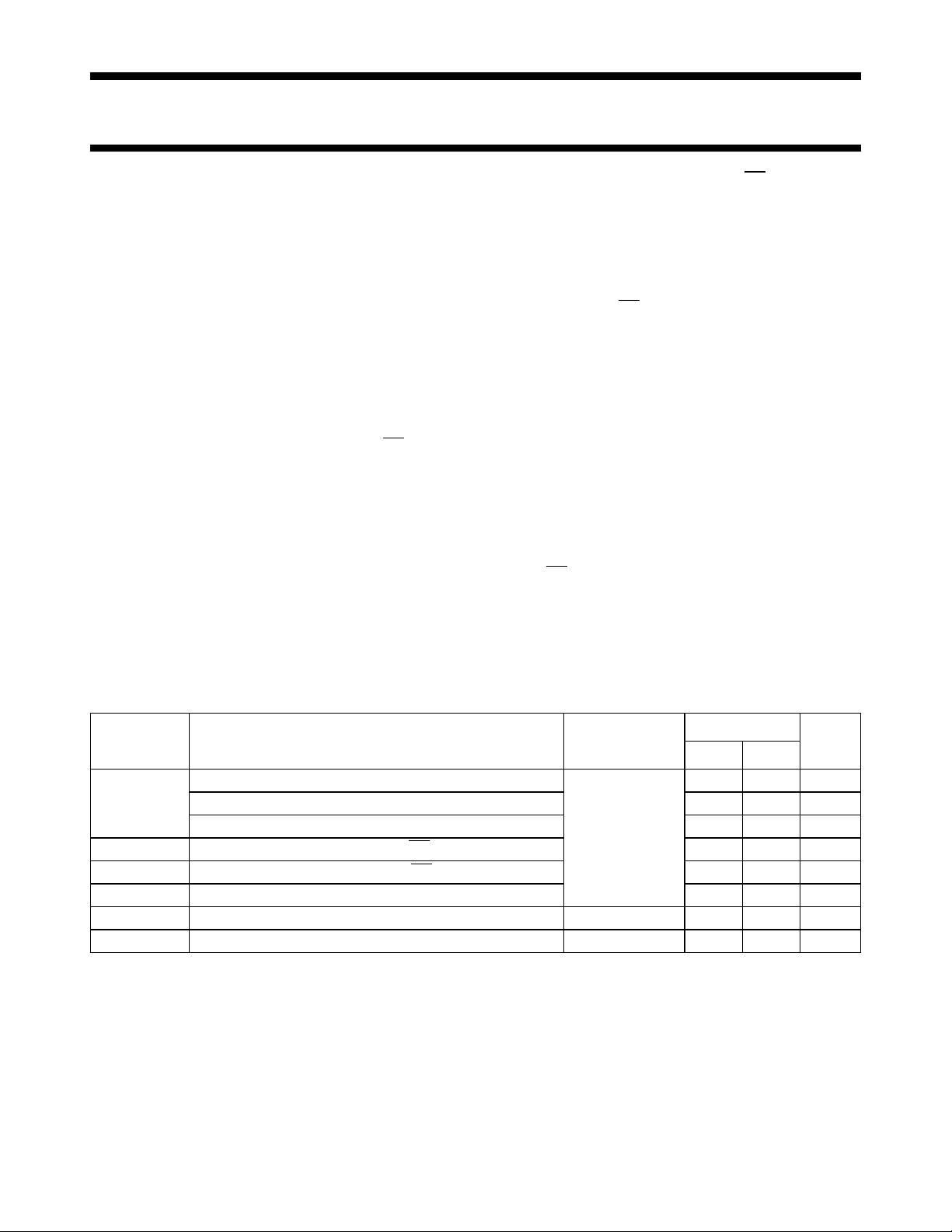
QUICK REFERENCE DATA
GND = 0 V; T
=25°C; tr=tf= 6 ns; VCC= 4.5 V; CL= 50 pF.
amb
SYMBOL PARAMETER CONDITIONS
t
PLH/tPZL
t
PHZ/tPZL
t
PHZ/tPLZ
f
max
C
I
C
PD
propagation delay An/Bnto Bn/A
propagation delay CP
propagation delay S
/CPBAto Bn/A
AB
AB/SBA
n
to Bn/A
n
n
3-state output enable time OEAB/OEBAto Bn/A
3-state output disable time OEAB/OEBAto Bn/A
n
n
CL= 15 pF;
VCC=5 V
maximum clock frequency 92 92 MHz
input capacitance 3.5 3.5 pF
power dissipation capacitance per channel notes 1 and 2 26 28 pF
Notes
1. C
is used to determine the dynamic power dissipation (PD in µW):
PD
PD=CPD× V
2
× fi+ ∑ (CL× V
CC
2
× fo) where:
CC
fi= input frequency in MHz; CL= output load capacitance in pF;
fo= output frequency in MHz; VCC= supply voltage in V;
∑ (CL× V
2. For HC the condition is VI= GND to V
2
× fo) = sum of the outputs
CC
CC
For HCT the condition is VI= GND to VCC− 1.5 V
TYPICAL
UNIT
HC HCT
13 13 ns
18 20 ns
20 23 ns
14 15 ns
12 13 ns
September 1993 2

Philips Semiconductors Product specification
Octal bus transceiver/register; 3-state 74HC/HCT652
ORDERING AND PACKAGE INFORMATION
TYPE NUMBER
PACKAGE
PINS PIN POSITION MATERIAL CODE
74HC/HCT652N 24 DIL plastic SOT101L
74HC/HCT652D 24 SO plastic SOT137A
PINNING
SYMBOL PIN DESCRIPTION
CP
S
OE
A
AB
0
AB
AB
..A
7
1 A to B clock input
2 select A to B source input
3 output enable A to B input
4..11 A data inputs/outputs
GND 12 ground (0 V)
B
OE
S
CP
V
7
BA
CC
..B
BA
BA
0
13..20 B data inputs/outputs
21 output enable B to A input
22 select B to A source input
23 B to A clock input
24 positive supply voltage
Fig.1 Pin configuration. Fig.2 Logic symbol. Fig.3 IEC logic symbol.
September 1993 3
 Loading...