

Philips 74hc hct595 DATASHEETS

INTEGRATED CIRCUITS
DATA SH EET
For a complete data sheet, please also download:
•The IC06 74HC/HCT/HCU/HCMOS Logic Family Specifications
•The IC06 74HC/HCT/HCU/HCMOS Logic Package Information
•The IC06 74HC/HCT/HCU/HCMOS Logic Package Outlines
74HC/HCT595
8-bit serial-in/serial or parallel-out
shift register with output latches;
3-state
Product specification
Supersedes data of September 1993
File under Integrated Circuits, IC06
1998 Jun 04
Philips Semiconductors Product specification
8-bit serial-in/serial or parallel-out shift
register with output latches; 3-state
FEATURES
• 8-bit serial input
• 8-bit serial or parallel output
• Storage register with 3-state outputs
• Shift register with direct clear
• 100 MHz (typ) shift out frequency
• Output capability:
– parallel outputs; bus driver
– serial output; standard
• ICC category: MSI.
APPLICATIONS
• Serial-to-parallel data conversion
• Remote control holding register.
74HC/HCT595
DESCRIPTION
The 74HC/HCT595 are high-speed Si-gate CMOS devices
and are pin compatible with low power Schottky TTL
(LSTTL). They are specified in compliance with JEDEC
standard no. 7A.
The “595” is an 8-stage serial shift register with a storage
register and 3-state outputs. The shift register and storage
register have separate clocks.
Data is shifted on the positive-going transitions of the
SHCP input. The data in each register is transferred to the
storage register on a positive-going transition of the ST
input. If both clocks are connected together, the shift
register will always be one clock pulse ahead of the
storage register.
The shift register has a serial input (DS) and a serial
standard output (Q7’) for cascading. It is also provided with
asynchronous reset (active LOW) for all 8 shift register
stages. The storage register has 8 parallel 3-state bus
driver outputs. Data in the storage register appears at the
output whenever the output enable input (OE) is LOW.
CP
QUICK REFERENCE DATA
GND = 0 V; T
=25°C; tr=tf= 6 ns.
amb
SYMBOL PARAMETER CONDITIONS
HC HCT
t
PHL/tPLH
propagation delay CL= 15 pF; VCC=5V
SH
to Q7’ 1621ns
CP
to Q
ST
CP
n
17 20 ns
MR to Q7’ 1419ns
f
max
C
I
C
PD
maximum clock frequency SHCP, ST
CP
100 57 MHz
input capacitance 3.5 3.5 pF
power dissipation capacitance per package notes 1 and 2 115 130 pF
Notes
1. C
is used to determine the dynamic power dissipation (PD in µW):
PD
PD=CPD× V
2
× fi+∑ (CL× V
CC
2
× fo) where:
CC
fi= input frequency in MHz
fo= output frequency in MHz
∑(CL× V
2
× fo) = sum of outputs
CC
CL= output load capacitance in pF
VCC= supply voltage in V
2. For HC the condition is VI= GND to VCC; for HCT the condition is VI= GND to VCC− 1.5 V.
TYP.
UNIT
1998 Jun 04 2

Philips Semiconductors Product specification
8-bit serial-in/serial or parallel-out shift
74HC/HCT595
register with output latches; 3-state
ORDERING INFORMATION
TYPE NUMBER
NAME DESCRIPTION VERSION
74HC595N DIP16 plastic dual in-line package; 16 leads (300 mil); long body SOT38-1
74HC595D SO16 plastic small outline package; 16 leads; body width 3.9 mm SOT109-1
74HC595DB SSOP16 plastic shrink small outline package; 16 leads; body width 5.3 mm SOT338-1
74HC595PW TSSOP16 plastic thin shrink small outline package; 16 leads; body width 4.4 mm SOT403-1
74HCT595N DIP16 plastic dual in-line package; 16 leads (300 mil); long body SOT38-1
74HCT595D SO16 plastic small outline package; 16 leads; body width 3.9 mm SOT109-1
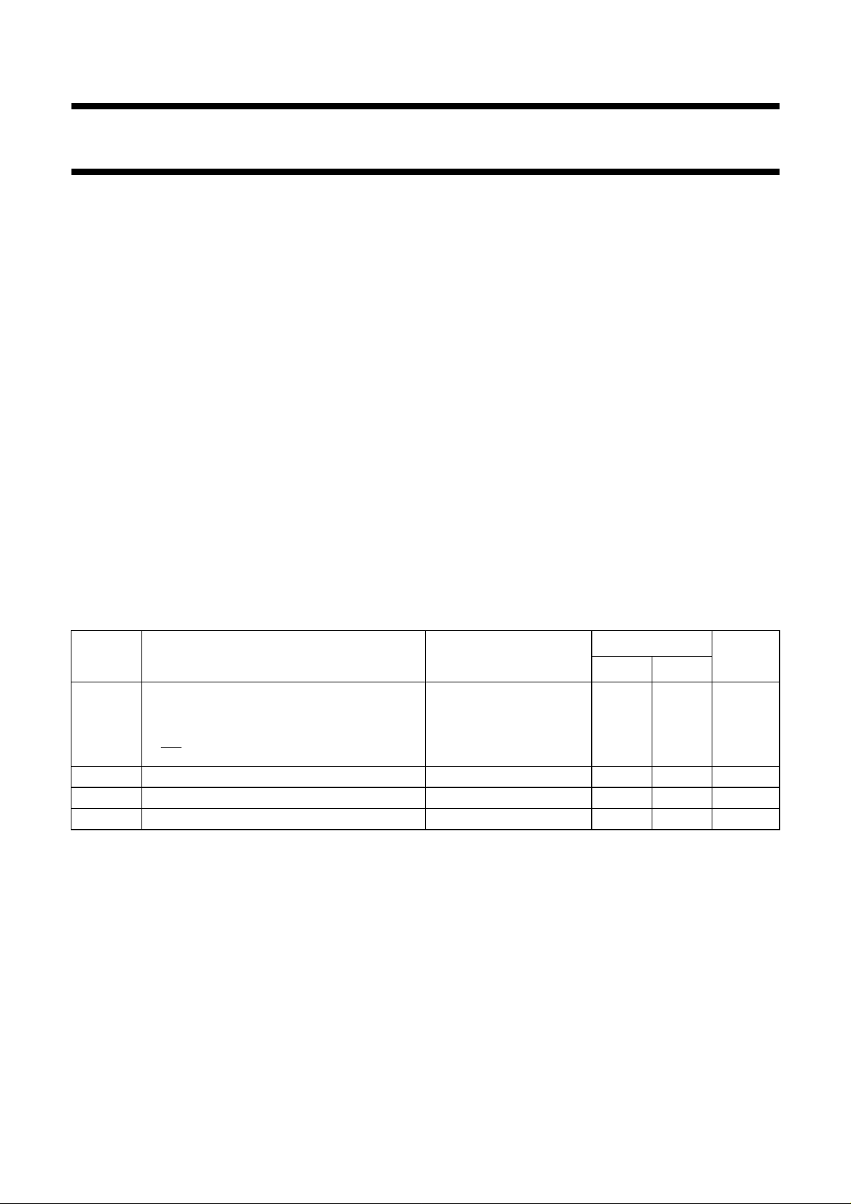
PINNING
SYMBOL PIN DESCRIPTION
Q
0
to Q
7
15, 1 to 7 parallel data output
GND 8 ground (0 V)
’ 9 serial data output
Q
7
MR 10 master reset (active LOW)
SH
CP
ST
CP
OE 13 output enable (active LOW)
D
S
V
CC
PACKAGE
11 shift register clock input
12 storage register clock input
14 serial data input
16 positive supply voltage
handbook, halfpage
Q
Q
Q
Q
Q
Q
Q
GND
1
1
2
2
3
3
4
4
5
6
7
595
5
6
7
8
MLA001
16
V
CC
Q
15
0
D
14
S
OE
13
ST
12
CP
SH
11
CP
MR
10
Q7'
9
Fig.1 Pin configuration.
1998 Jun 04 3
handbook, halfpage
11 12
SH
ST
CP
CP
Q7'
Q
0
Q
1
Q
14
D
S
2
Q
3
Q
4
Q
5
Q
6
Q
7
OEMR
1310
Fig.2 Logic symbol.
9
15
1
2
3
4
5
6
7
MLA002
Philips Semiconductors Product specification
8-bit serial-in/serial or parallel-out shift
register with output latches; 3-state
ST
SH
OE
CP
MR
CP
D
13
12
10
R
11
14
S
SRG8
C1/
1D 2D
Fig.3 IEC logic symbol.
handbook, halfpage
EN3
C2
3
MSA698
74HC/HCT595
15
Q
0
1
Q
1
2
Q
2
3
Q
3
4
Q
4
5
Q
5
6
Q
6
7
Q
7
9
Q7'
handbook, full pagewidth
D
14
S
SH
CP
11
MR
10
ST
12
OE
13
8-STAGE SHIFT REGISTER
CP
8-BIT STORAGE REGISTER
3-STATE OUTPUTS
Q7'
Q
0
Q
1
Q
2
Q
3
Q
4
Q
5
Q
6
Q
7
MLA003
9
15
1
2
3
4
5
6
7
Fig.4 Functional diagram.
1998 Jun 04 4

Philips Semiconductors Product specification
8-bit serial-in/serial or parallel-out shift
register with output latches; 3-state
handbook, full pagewidth
D
S
SH
CP
MR
STAGE 0 STAGES 1 TO 6 STAGE 7
DCPQ
FF0
R
DCPQ
LATCH
DQ
DCPQ
FF7
R
DCPQ
LATCH
74HC/HCT595
Q
'
7
ST
CP
OE
Q
0
Q
Q
1
2
Fig.5 Logic diagram.
Q
Q
Q
3
Q
4
5
6
Q
MLA010
7
1998 Jun 04 5
Philips Semiconductors Product specification
8-bit serial-in/serial or parallel-out shift
74HC/HCT595
register with output latches; 3-state
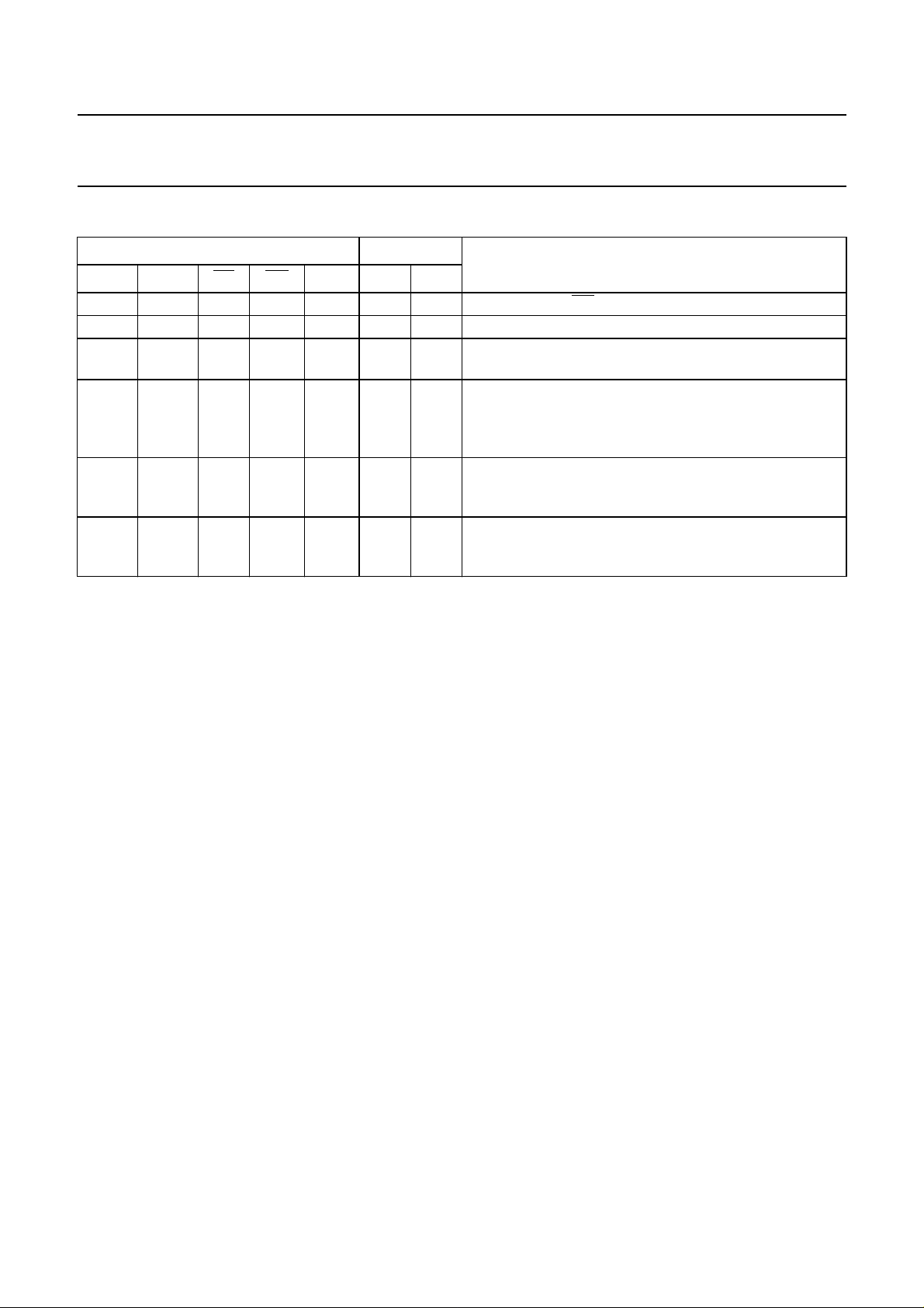
FUNCTION TABLE
INPUTS OUTPUTS
SH
CP
ST
OE MR D
CP
Q7’Q
S
N
X X L L X L NC a LOW level on MR only affects the shift registers
X ↑ L L X L L empty shift register loaded into storage register
X X H L X L Z shift register clear. Parallel outputs in high-impedance
OFF-state
↑ XLHHQ
’ NC logic high level shifted into shift register stage 0. Contents
6
of all shift register stages shifted through, e.g. previous
state of stage 6 (internal Q
(Q7’)
X ↑ LHXNCQ
’ contents of shift register stages (internal Qn’) are
n
transferred to the storage register and parallel output
stages
↑↑LHXQ
’Qn’ contents of shift register shifted through. Previous
6
contents of the shift register is transferred to the storage
register and the parallel output stages.
FUNCTON
’) appears on the serial output
6
Notes
1. H = HIGH voltage level; L = LOW voltage level
↑ = LOW-to-HIGH transition; ↓ = HIGH-to-LOW transition
Z = high-impedance OFF-state; NC = no change
X = don’t care.
1998 Jun 04 6
 Loading...