

Philips 74hc hct4543 DATASHEETS

INTEGRATED CIRCUITS
DATA SH EET
For a complete data sheet, please also download:
•The IC06 74HC/HCT/HCU/HCMOS Logic Family Specifications
•The IC06 74HC/HCT/HCU/HCMOS Logic Package Information
•The IC06 74HC/HCT/HCU/HCMOS Logic Package Outlines
74HC/HCT4543
BCD to 7-segment
latch/decoder/driver for LCDs
Product specification
File under Integrated Circuits, IC06
December 1990
Philips Semiconductors Product specification
BCD to 7-segment latch/decoder/driver
for LCDs
FEATURES
• Latch storage of BCD inputs
• Blanking inputs
• Output capability: non-standard
• ICC category: MSI
GENERAL DESCRIPTION
The 74HC/HCT4543 are high-speed Si-gate CMOS
devices and are pin compatible with “4543” of the “4000B”
series. They are specified in compliance with JEDEC
standard no. 7A.
The 74HC/HCT4543 are BCD to 7-segment
latch/decoder/drivers for liquid crystal displays. They have
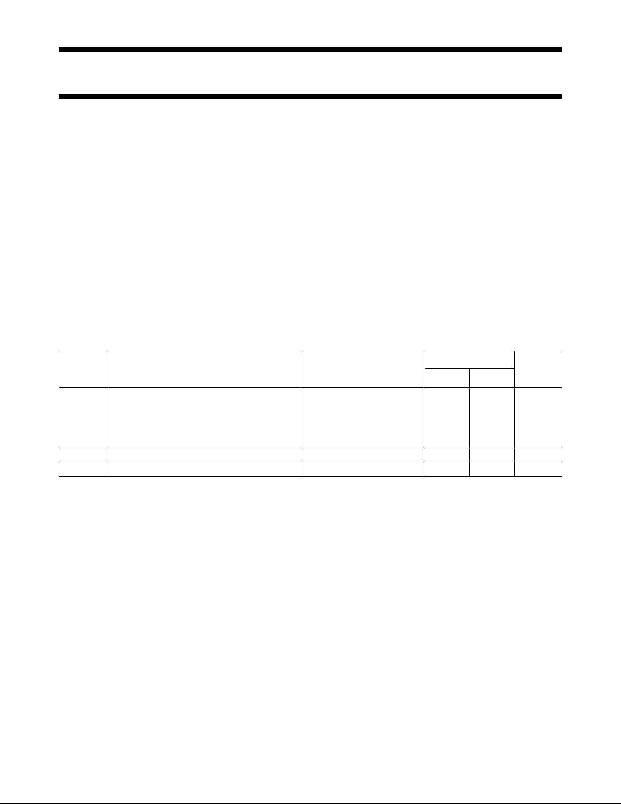
QUICK REFERENCE DATA
GND = 0 V; T
=25°C; tr=tf=6ns
amb
SYMBOL PARAMETER CONDITIONS
t
PHL
C
C
/ t
I
PD
propagation delay CL= 15 pF; VCC=5V
PLH
D
to Q
n
n
LD to Q
BI to Q
n
n
input capacitance 3.5 3.5 pF
power dissipation capacitance per package notes 1 and 2 42 42 pF
four address inputs (D
disable input (LD), an active HIGH blanking input (BI), an
active HIGH phase input (PH) and seven buffered
segment outputs (Qato Qg).
The “4543” provides the function of a 4-bit storage latch
and an 8-4-2-1 BCD to 7-segment decoder driver. The
“4543” can invert the logic levels of the output combination.
The phase (PH), blanking (BI) and latch disable (LD)
inputs are used to reverse the function table phase, blank
the display and store a BCD code, respectively.
For liquid crystal displays a square-wave is applied to PH
and the electrical common back-plane of the display. The
outputs of the “4543” are directly connected to the
segments of the liquid crystal.
74HC/HCT4543
to D3), an active HIGH latch
0
TYPICAL
HC HCT
29 33 ns
32 31 ns
20 28 ns
UNIT
Notes
1. C
is used to determine the dynamic power dissipation (PD in µW):
PD
PD=CPD× V
2
× fi+∑ (CL× V
CC
2
× fo) where:
CC
fi= input frequency in MHz
fo= output frequency in MHz
∑ (CL× V
2
× fo) = sum of outputs
CC
CL= output load capacitance in pF
VCC= supply voltage in V
2. For HC the condition is VI= GND to V
CC
For HCT the condition is VI= GND to VCC−1.5 V
ORDERING INFORMATION
“74HC/HCT/HCU/HCMOS Logic Package Information”
See
December 1990 2
.

Philips Semiconductors Product specification
BCD to 7-segment latch/decoder/driver for
LCDs
PIN DESCRIPTION
PIN NO. SYMBOL NAME AND FUNCTION
1 LD latch disable input (active HIGH)
5, 3, 2, 4 D
6 PH phase input (active HIGH)
7 BI blanking input (active HIGH)
8 GND ground (0 V)
9, 10, 11, 12, 13, 15, 14 Q
16 V
to D
0
to Q
a
CC
3
g
address (data) inputs
segment outputs
positive supply voltage
74HC/HCT4543
Fig.1 Pin configuration. Fig.2 Logic symbol. Fig.3 IEC logic symbol.
December 1990 3

Philips Semiconductors Product specification
BCD to 7-segment latch/decoder/driver for
74HC/HCT4543
LCDs
APPLICATIONS
• Driving LCD displays
• Driving fluorescent displays
• Driving incandescent displays
• Driving gas discharge displays
Fig.4 Functional diagram. Fig.5 Segment designation.
FUNCTION TABLE
INPUTS OUTPUTS DISPLAY
LD BI PH
X H L X X X X L L L L L L L blank
H
H
H
H
H
H
H
H
H
H
H
H
H
H
H
H
L
L
L
L
L
L
L
L
L
L
L
L
L
L
L
L
LLL XXXX
as
above
(1)
D
D
D
D
3
2
1
L
L
L
L
L
L
L
L
L
L
L
L
L
L
L
L
L
L
L
L
L
L
L
L
H
H
H
H
H
H
H
H
L
L
L
L
L
H
L
H
L
L
H
H
H
L
L
H
L
H
H
H
L
H
H
H
L
L
L
L
L
H
L
H
L
L
H
H
H
L
L
H
L
H
H
H
L
H
H
H
Q
0
H
L
H
H
L
H
H
H
H
H
L
L
L
L
L
L
Q
a
H
H
H
H
H
L
L
H
H
H
L
L
L
L
L
L
Q
Q
b
c
H
H
L
H
H
H
H
H
H
H
L
L
L
L
L
L
H
L
H
H
L
H
H
L
H
H
L
L
L
L
L
L
(1) (1)
Q
d
H
L
H
L
L
L
H
L
H
L
L
L
L
L
L
L
H as above inverse of above
Q
e
H
L
L
L
H
H
H
L
H
H
L
L
L
L
L
L
Q
f
g
L
L
H
H
H
H
H
L
H
H
L
L
L
L
L
L
0
1
2
3
4
5
6
7
8
9
blank
blank
blank
blank
blank
blank
as
above
Notes
1. For liquid crystal displays, apply a square-wave to PH.
2. Depends upon the BCD-code previously applied when LD = HIGH.
H = HIGH voltage level
L = LOW voltage level
X = don’t care
December 1990 4
 Loading...