

Philips 74hc hct4538 DATASHEETS

INTEGRATED CIRCUITS
DATA SH EET
For a complete data sheet, please also download:
•The IC06 74HC/HCT/HCU/HCMOS Logic Family Specifications
•The IC06 74HC/HCT/HCU/HCMOS Logic Package Information
•The IC06 74HC/HCT/HCU/HCMOS Logic Package Outlines
74HC/HCT4538
Dual retriggerable precision
monostable multivibrator
Product specification
File under Integrated Circuits, IC06
September 1993
Philips Semiconductors Product specification
Dual retriggerable precision monostable
multivibrator
FEA TURES
• Separate reset inputs
• Triggering from leading or trailing edge
• Output capability: standard
• ICC category: MSI
• Power-on reset on-chip
GENERAL DESCRIPTION
The 74HC/HCT4538 are high-speed Si-gate CMOS
devices and are pin compatible with “4538” of the “4000B”
series. They are specified in compliance with JEDEC
standard no. 7A.
The 74HC/HCT4538 are dual retriggerable-resettable
monostable multivibrators. Each multivibrator has an
active LOW trigger/retrigger input (n
QUICK REFERENCE DATA
GND = 0 V; T
= 25 °C; tr= tf= 6 ns
amb
A0), an active HIGH
74HC/HCT4538
trigger/retrigger input (nA1) , an overriding active LOW
direct reset input (nRD), an output (nQ) and its complement
(nQ), and two pins (nCTCand nRCTC) for connecting the
external timing components Ctand Rt. Typical pulse width
variation over temperature range is ± 0.2%.
The “4538” may be triggered by either the positive or the
negative edges of the input pulse. The duration and
accuracy of the output pulse are determined by the
external timing components Ctand Rt. The output pulse
width (T) is equal to 0.7 × Rt× Ct. The linear design
techniques guarantee precise control of the output pulse
width.
A LOW level at nRDterminates the output pulse
immediately.
Schmitt-trigger action in the trigger inputs makes the circuit
highly tolerant to slower rise and fall times.
SYMBOL PARAMETER CONDITIONS
t
PHL
C
C
I
PD
/ t
PLH
propagation delay nA0,nA1to nQ, nQC
= 15 pF; VCC= 5 V 27 30 ns
L
input capacitance 3.5 3.5 pF
power dissipation capacitance per multivibrator notes 1 and 2 136 138 pF
Notes
1. C
is used to determine the dynamic power dissipation (PDin µW):
PD
PD= CPD× V
+ 0.48 × C
EXT
2
× fi+∑(CL× V
CC
2
× V
× fo+ D × 0.8 × VCCwhere:
CC
CC
2
× fo) +
fi= input frequency in MHz
fo= output frequency in MHz
∑ (CL× V
2
× fo) = sum of outputs
CC
CL= output load capacitance in pF
VCC= supply voltage in V
D = duty factor in %
C
= timing capacitance in pF
EXT
2. For HC the condition is VI= GND to V
CC
For HCT the condition is VI= GND to VCC− 1.5 V
TYPICAL
UNIT
HC HCT
ORDERING INFORMATION
“74HC/HCT/HCU/HCMOS Logic Package Information”
See
September 1993 2
.
Philips Semiconductors Product specification
Dual retriggerable precision monostable
multivibrator
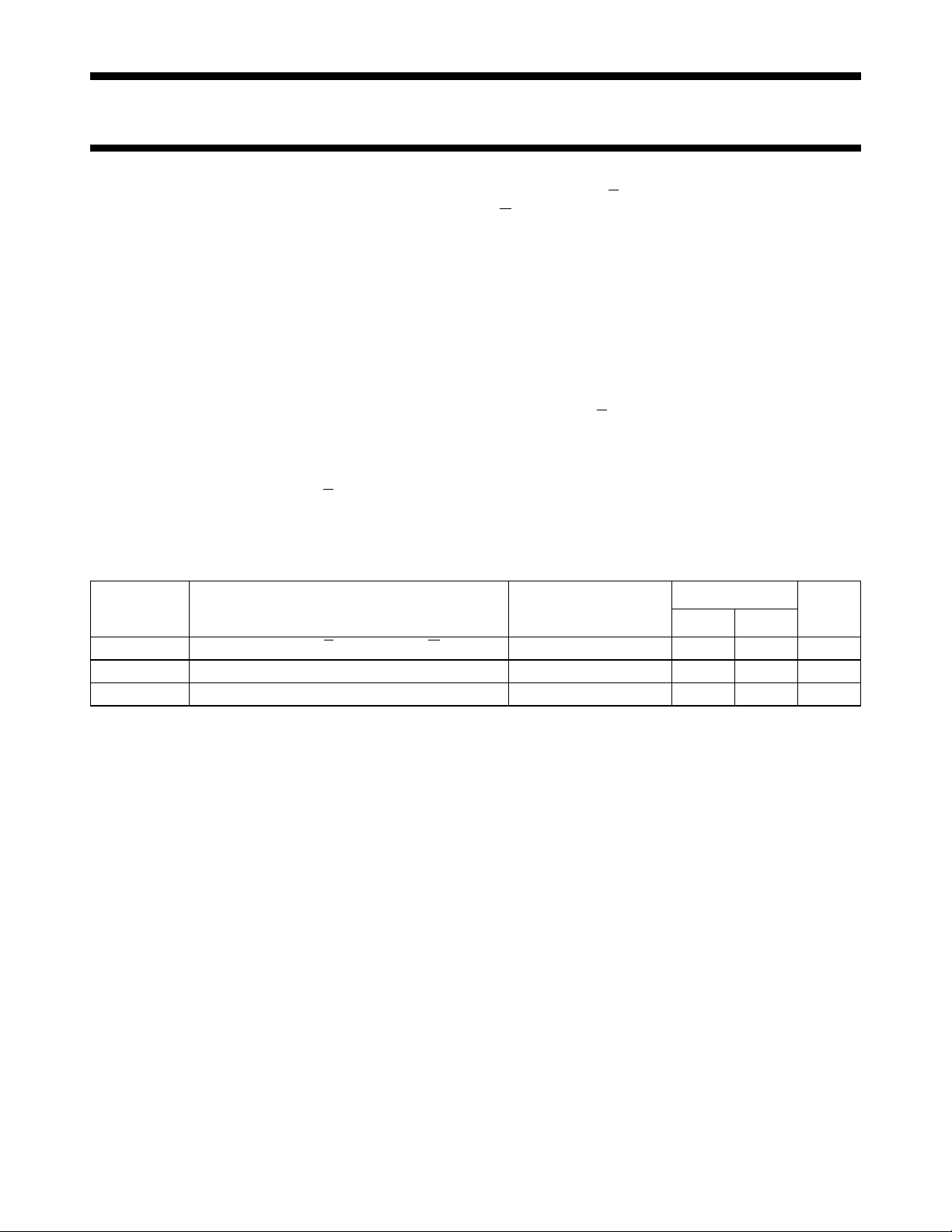
PIN DESCRIPTION
PIN NO. SYMBOL NAME AND FUNCTION
1, 15 1C
2, 14 1RC
3, 13 1
4, 12 1A
5, 11 1
6, 10 1Q, 2Q pulse outputs
7, 9 1
8 GND ground (0 V)
16 V
,2C
TC
, 2RC
TC
RD,2R
,2A
1
A0,2A
TC
D
1
0
external capacitor connections
external resistor/capacitor connections
TC
direct reset inputs (active LOW)
trigger inputs (LOW-to-HIGH, edge-triggered)
trigger inputs (HIGH-to-LOW, edge-triggered)
Q, 2Q complementary pulse outputs
CC
positive supply voltage
74HC/HCT4538
Fig.1 Pin configuration. Fig.2 Logic symbol. Fig.3 IEC logic symbol.
September 1993 3

Philips Semiconductors Product specification
Dual retriggerable precision monostable
multivibrator
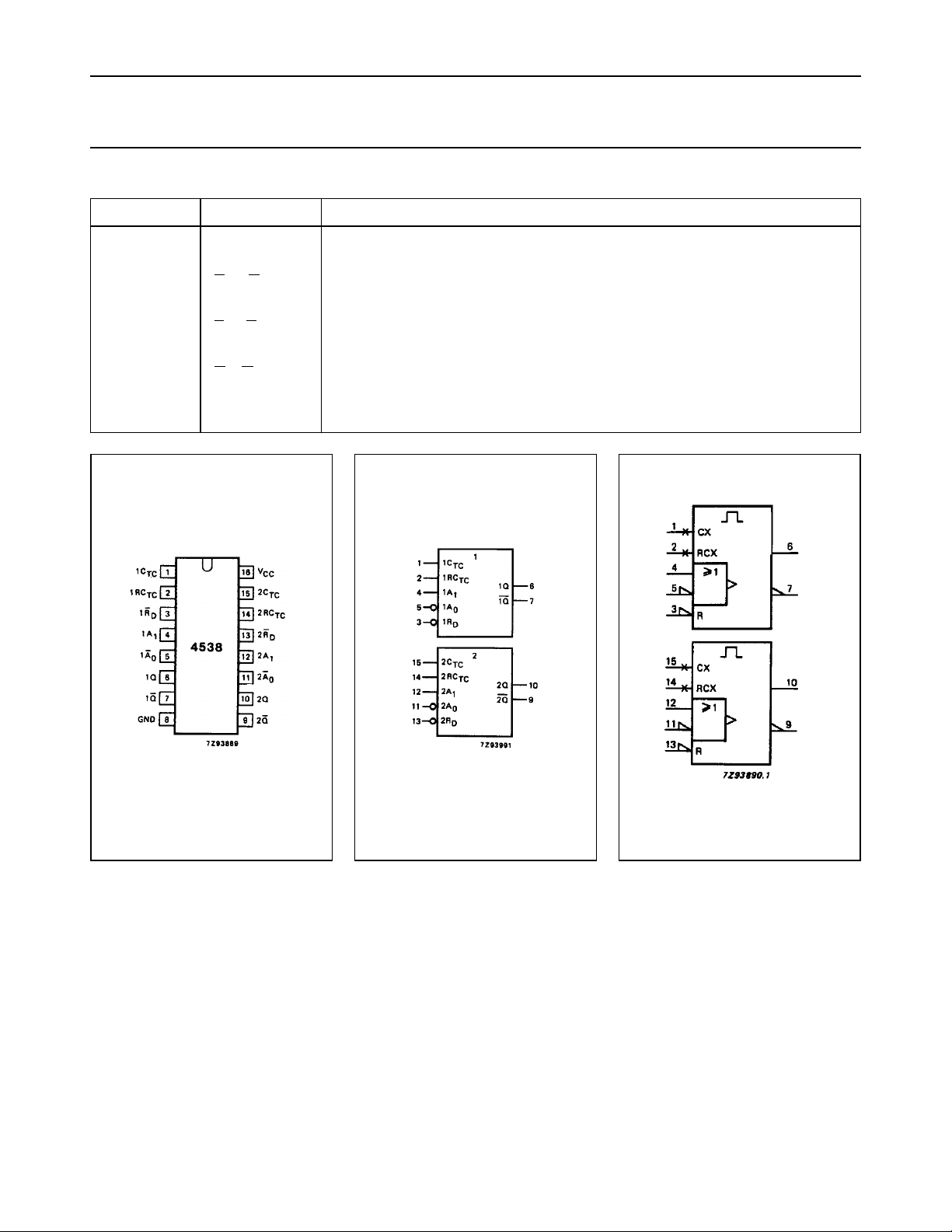
Fig.4 Functional diagram.
74HC/HCT4538
FUNCTION TABLE
INPUTS OUTPUTS
nA
0
↓ LH
H↑H
XXL LH
Notes
1. H = HIGH voltage level
L = LOW voltage level
X = don’t care
↑ = LOW-to-HIGH transition
↓ = HIGH-to-LOW transition
nA
1
nR
D
nQ nQ
= one HIGH level output pulse
= one LOW level output pulse
(1) Connect CTC(pins 1 and 15) to GND (pin 8).
Fig.5 Connection of the external timing
components Rtand Ct.
(1) Positive edge triggering.
(2) Positive edge retriggering (pulse
lengthening).
(3) Negative edge triggering.
(4) Reset (pulse shortening).
and V
(5) V
ref1
(6) T = 0.7 × Rt× Ct(see also Fig.5).
are internal reference voltages.
ref2
Fig.6 Timing diagram.
September 1993 4
 Loading...