

Philips 74hc hct4067 DATASHEETS
INTEGRATED CIRCUITS
DATA SH EET
For a complete data sheet, please also download:
•The IC06 74HC/HCT/HCU/HCMOS Logic Family Specifications
•The IC06 74HC/HCT/HCU/HCMOS Logic Package Information
•The IC06 74HC/HCT/HCU/HCMOS Logic Package Outlines
74HC/HCT4067
16-channel analog
multiplexer/demultiplexer
Product specification
File under Integrated Circuits, IC06
September 1993
Philips Semiconductors Product specification
16-channel analog
multiplexer/demultiplexer
FEATURES
• Low “ON” resistance:
80 Ω (typ.) at VCC= 4.5 V
70 Ω (typ.) at VCC= 6.0 V
60 Ω (typ.) at VCC= 9.0 V
typical “break before make” built-in
• Output capability: non-standard
• ICC category: MSI
GENERAL DESCRIPTION
The 74HC/HCT4067 are high-speed Si-gate CMOS
devices and are pin compatible with the “4067” of the
“4000B” series. They are specified in compliance with
JEDEC standard no. 7A.
QUICK REFERENCE DATA
GND = 0 V; T
= 25 °C; tr= tf= 6 ns
amb
74HC/HCT4067
The 74HC/HCT4067 are 16-channel analog
multiplexers/demultiplexers with four address inputs (S
S3) , an active LOW enable input (E), sixteen independent
inputs/outputs (Y0to Y15) and a common input/output (Z).
The ”4067” contains sixteen bidirectional analog switches,
each with one side connected to an independent
input/output (Y0to Y15) and the other side connected to a
common input/output (Z).
With E LOW, one of the sixteen switches is selected (low
impedance ON-state) by S0to S3. All unselected switches
are in the high impedance OFF-state. With E HIGH, all
switches are in the high impedance OFF-state,
independent of S0to S3.
The analog inputs/outputs (Y0to Y15, and Z) can swing
between VCCas a positive limit and GND as a negative
limit. VCCto GND may not exceed 10 V.
0
to
SYMBOL PARAMETER CONDITIONS
t
t
C
C
C
PZL
PLZ
I
PD
S
/ t
/ t
turn-on time CL= 15 pF; RL=1 kΩ; VCC= 5 V
PZH
E to V
os
S
to V
n
os
turn-off time
PHZ
E to V
os
to V
S
n
os
input capacitance 3.5 3.5 pF
power dissipation capacitance per switch notes 1 and 2 29 29 pF
max. switch capacitance
independent (Y) 5 5 pF
common (Z) 45 45 pF
Notes
1. C
is used to determine the dynamic power dissipation (PDin µW):
PD
PD= CPD× V
2
× fi+∑{(CL+ CS) × V
CC
2
× fo} where:
CC
fi= input frequency in MHz
fo= output frequency in MHz
∑ {(CL+ CS) × V
2
× fo} = sum of outputs
CC
CL= output load capacitance in pF
CS= max. switch capacitance in pF
VCC= supply voltage in V
2. For HC the condition is VI= GND to V
CC
For HCT the condition is VI= GND to VCC− 1.5 V
TYPICAL
UNIT
HC HCT
26 32 ns
29 33 ns
27 26 ns
29 30 ns
September 1993 2
Philips Semiconductors Product specification
16-channel analog
multiplexer/demultiplexer
ORDERING INFORMATION
See
“74HC/HCT/HCU/HCMOS Logic Package Information”
PIN DESCRIPTION
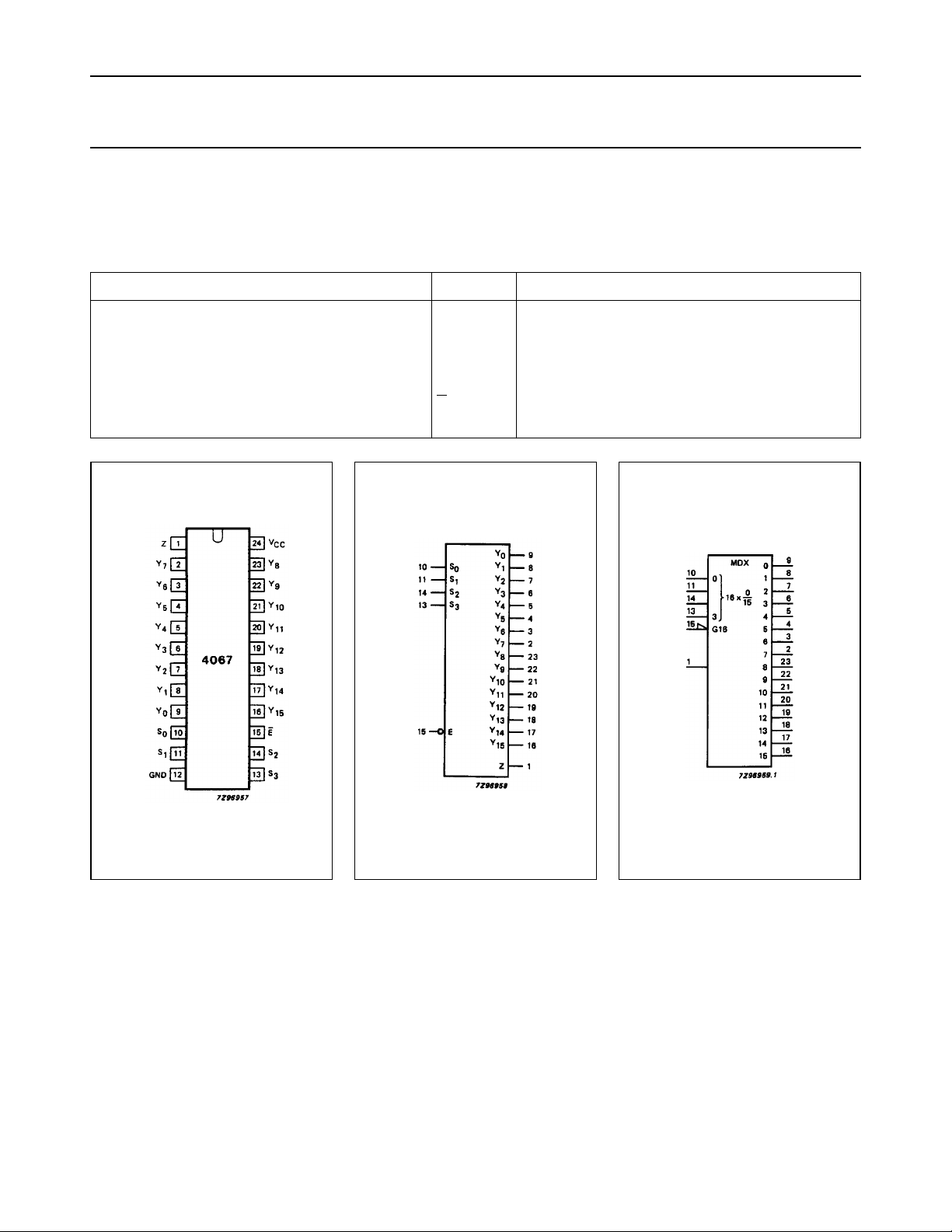
PIN NO. SYMBOL NAME AND FUNCTION
1 Z common input/output
9, 8, 7, 6, 5, 4, 3, 2, 23, 22, 21, 20, 19, 18, 17, 16 Y
10, 11, 14, 13 S
12 GND ground (0 V)
15
24 V
.
to Y
0
to S
0
E enable input (active LOW)
CC
independent inputs/outputs
15
address inputs
3
positive supply voltage
74HC/HCT4067
Fig.1 Pin configuration. Fig.2 Logic symbol. Fig.3 IEC logic symbol.
September 1993 3
Philips Semiconductors Product specification
16-channel analog
multiplexer/demultiplexer
APPLICATIONS
• Analog multiplexing and demultiplexing
• Digital multiplexing and demultiplexing
• Signal gating
Fig.4 Functional diagram.
74HC/HCT4067
FUNCTION TABLE
INPUTS CHANNEL
ES
L
L
L
L
L
L
L
L
L
L
L
L
L
L
L
L
L
L
L
L
L
L
L
L
H
H
H
H
H
H
H
H
H X X X X none
3
S
2
L
L
L
L
H
H
H
H
L
L
L
L
H
H
H
H
S
1
L
L
H
H
L
L
H
H
L
L
H
H
L
L
H
H
S
0
L
H
L
H
L
H
L
H
L
H
L
H
L
H
L
H
ON
Y
−Z
0
Y
−Z
1
Y
−Z
2
Y
−Z
3
−Z
Y
4
Y
−Z
5
Y
−Z
6
Y
−Z
7
−Z
Y
8
Y
−Z
9
Y10− Z
Y11− Z
Y
− Z
12
Y13− Z
Y14− Z
Y15− Z
Fig.5 Schematic diagram (one switch).
September 1993 4
Notes
1. H = HIGH voltage level
L = LOW voltage level
X = don’t care
Philips Semiconductors Product specification
16-channel analog
multiplexer/demultiplexer
74HC/HCT4067
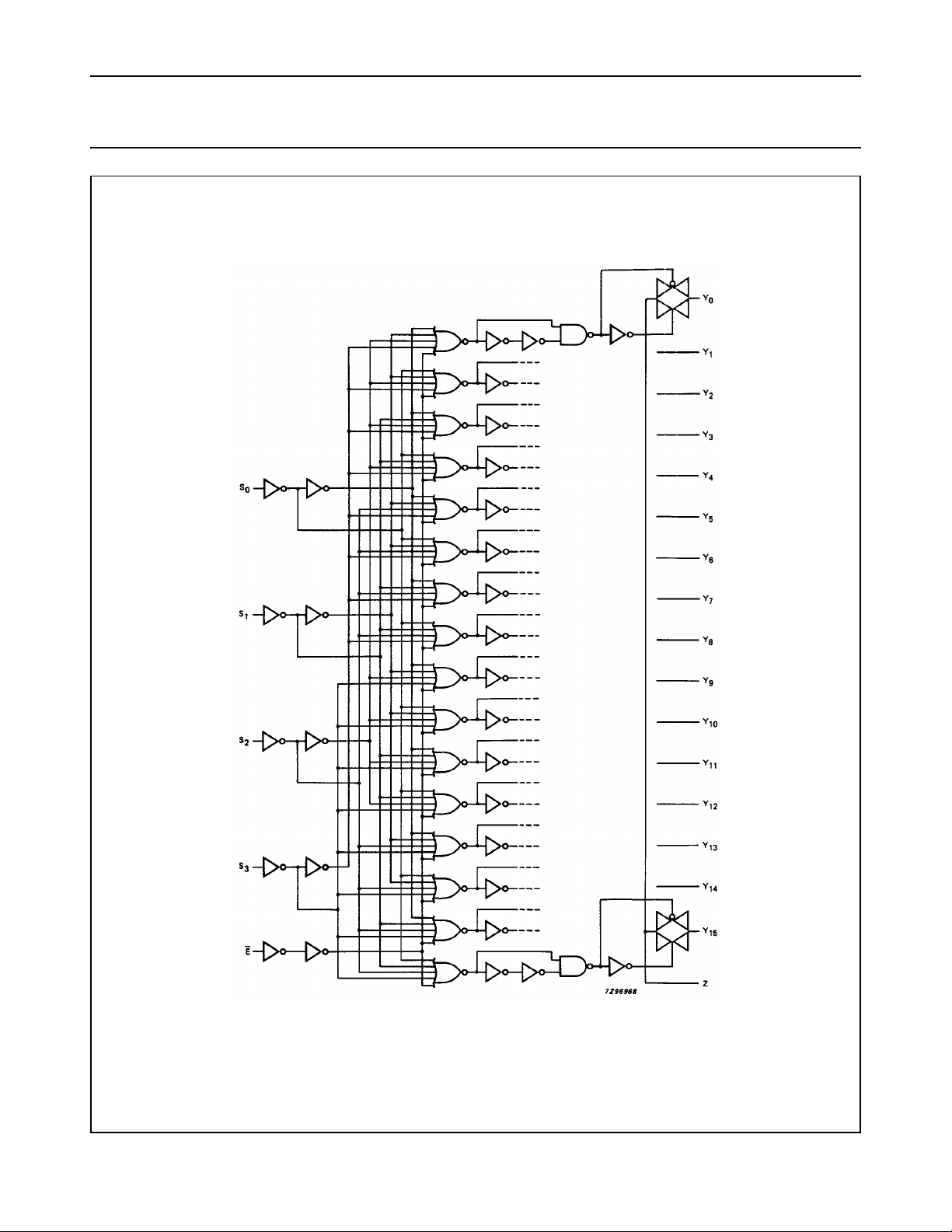
Fig.6 Logic diagram.
September 1993 5
 Loading...