

Philips 74hc hct4040 DATASHEETS
INTEGRATED CIRCUITS
DATA SH EET
For a complete data sheet, please also download:
•The IC06 74HC/HCT/HCU/HCMOS Logic Family Specifications
•The IC06 74HC/HCT/HCU/HCMOS Logic Package Information
•The IC06 74HC/HCT/HCU/HCMOS Logic Package Outlines
74HC/HCT4040
12-stage binary ripple counter
Product specification
File under Integrated Circuits, IC06
December 1990
Philips Semiconductors Product specification
12-stage binary ripple counter 74HC/HCT4040
FEATURES
• Output capability: standard
• ICC category: MSI
GENERAL DESCRIPTION
The 74HC/HCT4040 are high-speed Si-gate CMOS
devices and are pin compatible with “4040” of the “4000B”
series. They are specified in compliance with JEDEC
standard no. 7A.
The 74HC/HCT4040 are 12-stage binary ripple counters
with a clock input (
CP), an overriding asynchronous
(Q0 to Q11). The counter advances on the HIGH-to-LOW
transition of CP.
A HIGH on MR clears all counter stages and forces all
outputs LOW, independent of the state of CP.
Each counter stage is a static toggle flip-flop.
APPLICATIONS
• Frequency dividing circuits
• Time delay circuits
• Control counters
master reset input (MR) and twelve parallel outputs
QUICK REFERENCE DATA
GND = 0 V; T
=25°C; tr=tf= 6 ns
amb
SYMBOL PARAMETER CONDITIONS
t
/ t
PHL
PLH
f
max
C
I
C
PD
propagation delay CL= 15 pF; VCC=5 V
CP to Q
Q
to Q
n
0
n+1
maximum clock frequency 90 79 MHz
input capacitance 3.5 3.5 pF
power dissipation capacitance per package notes 1 and 2 20 20 pF
TYPICAL
UNIT
HC HCT
14 16 ns
88ns
Notes
1. C
is used to determine the dynamic power dissipation (PD in µW):
PD
PD=CPD× V
2
× fi+∑(CL× V
CC
2
× fo) where:
CC
fi= input frequency in MHz
fo= output frequency in MHz
∑ (CL× V
2
× fo) = sum of outputs
CC
CL= output load capacitance in pF
VCC= supply voltage in V
2. For HC the condition is VI= GND to V
CC
For HCT the condition is VI= GND to VCC− 1.5 V
ORDERING INFORMATION
“74HC/HCT/HCU/HCMOS Logic Package Information”
See
.
December 1990 2
Philips Semiconductors Product specification
12-stage binary ripple counter 74HC/HCT4040
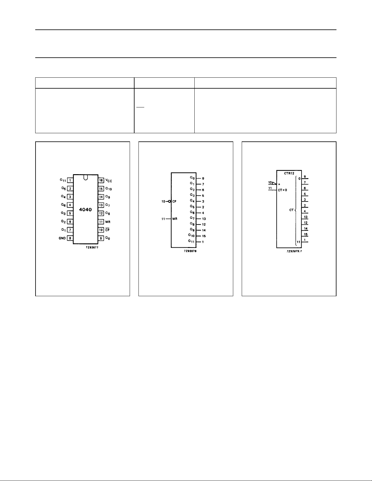
PIN DESCRIPTION
PIN NO. SYMBOL NAME AND FUNCTION
8 GND ground (0 V)
9, 7, 6, 5, 3, 2, 4, 13, 12, 14, 15, 1 Q
10
11 MR master reset input (active HIGH)
16 V
to Q
0
11
parallel outputs
CP clock input (HIGH-to-LOW, edge-triggered)
CC
positive supply voltage
Fig.1 Pin configuration. Fig.2 Logic symbol. Fig.3 IEC logic symbol.
December 1990 3
 Loading...