

Philips 74hc hct4024 DATASHEETS

INTEGRATED CIRCUITS
DATA SH EET
For a complete data sheet, please also download:
•The IC06 74HC/HCT/HCU/HCMOS Logic Family Specifications
•The IC06 74HC/HCT/HCU/HCMOS Logic Package Information
•The IC06 74HC/HCT/HCU/HCMOS Logic Package Outlines
74HC/HCT4024
7-stage binary ripple counter
Product specification
File under Integrated Circuits, IC06
December 1990
Philips Semiconductors Product specification
7-stage binary ripple counter 74HC/HCT4024
FEATURES
• Output capability: standard
• ICC category: MSI
GENERAL DESCRIPTION
The 74HC/HCT4024 are high-speed Si-gate CMOS
devices and are pin compatible with the “4024” of the
The counter advances on the HIGH-to-LOW transition of
CP.
A HIGH on MR clears all counter stages and forces all
outputs LOW, independent of the state of CP.
Each counter stage is a static toggle flip-flop.
Schmitt-trigger action in the clock input makes the circuit
highly tolerant to slower clock rise and fall times.
“4000B” series. They are specified in compliance with
JEDEC standard no. 7A.
The 74HC/HCT4024 are 7-stage binary ripple counters
with a clock input (
CP), an overriding asynchronous
master reset input (MR) and seven fully buffered parallel
APPLICATIONS
• Frequency dividing circuits
• Time delay circuits
outputs (Q0to Q6).
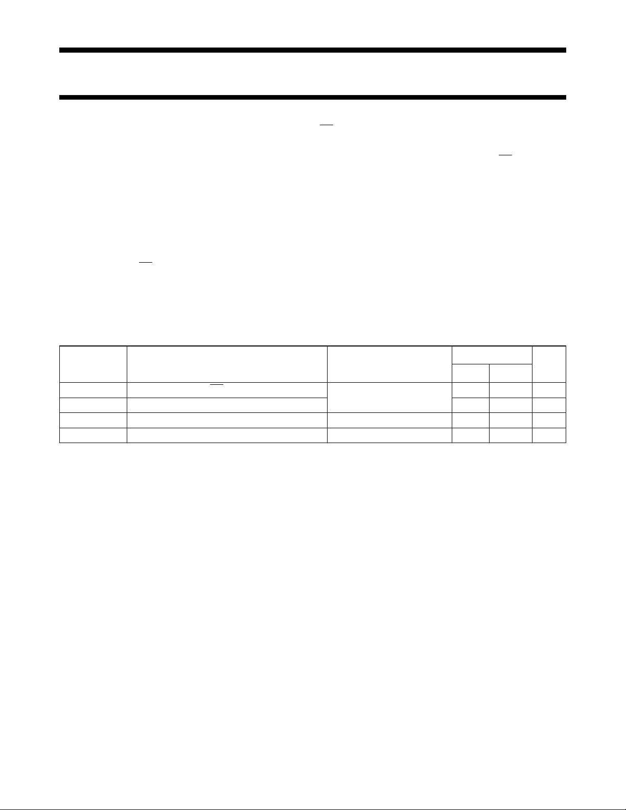
QUICK REFERENCE DATA
GND = 0 V; T
=25°C; tr=tf= 6 ns
amb
SYMBOL PARAMETER CONDITIONS
t
PHL
f
max
C
C
I
PD
/ t
PLH
propagation delay CP to Q
0
CL= 15 pF; VCC= 5 V 14 14 ns
maximum clock frequency 90 70 MHz
input capacitance 3.5 3.5 pF
power dissipation capacitance per package notes 1 and 2 25 27 pF
TYPICAL
UNIT
HC HCT
Notes
1. C
is used to determine the dynamic power dissipation (PD in µW):
PD
PD=CPD× V
2
× fi+∑ (CL× V
CC
2
× fo) where:
CC
fi= input frequency in MHz
fo= output frequency in MHz
∑ (CL× V
2
× fo) = sum of outputs
CC
CL= output load capacitance in pF
VCC= supply voltage in V
2. For HC the condition is VI= GND to V
CC
For HCT the condition is VI= GND to VCC− 1.5 V
ORDERING INFORMATION
See
“74HC/HCT/HCU/HCMOS Logic Package Information”
.
December 1990 2

Philips Semiconductors Product specification
7-stage binary ripple counter 74HC/HCT4024
PIN DESCRIPTION
PIN NO. SYMBOL NAME AND FUNCTION
1
2 MR master reset input (active HIGH)
12, 11, 9, 6, 5, 4, 3 Q
7 GND ground (0 V)
8, 10, 13 n.c. not connected
14 V
CP clock input (HIGH-to-LOW, edge-triggered)
to Q
0
CC
parallel outputs
6
positive supply voltage
Fig.1 Pin configuration. Fig.2 Logic symbol. Fig.3 IEC logic symbol.
December 1990 3
 Loading...