

Philips 74hc hct4016 DATASHEETS

INTEGRATED CIRCUITS
DATA SH EET
For a complete data sheet, please also download:
•The IC06 74HC/HCT/HCU/HCMOS Logic Family Specifications
•The IC06 74HC/HCT/HCU/HCMOS Logic Package Information
•The IC06 74HC/HCT/HCU/HCMOS Logic Package Outlines
74HC/HCT4016
Quad bilateral switches
Product specification
File under Integrated Circuits, IC06
December 1990
Philips Semiconductors Product specification
Quad bilateral switches 74HC/HCT4016
FEATURES
• Low “ON” resistance:
160 Ω (typ.) at VCC= 4.5 V
120 Ω (typ.) at VCC= 6.0 V
80 Ω (typ.) at VCC= 9.0 V
• Individual switch controls
• Typical “break before make” built in
• Output capability: non-standard
• ICC category: SSI
“4000B” series. They are specified in compliance with
JEDEC standard no. 7A.
The 74HC/HCT4016 have four independent analog
switches (transmission gates).
Each switch has two input/output terminals (Y
active HIGH enable input (En). When Enis connected to
VCC, a low bidirectional path between Ynand Znis
established (ON condition). When Enis connected to
ground (GND), the switch is disabled and a high
impedance between Ynand Znis established (OFF
condition).
Current through a switch will not cause additional
GENERAL DESCRIPTION
The 74HC/HCT4016 are high-speed Si-gate CMOS
devices and are pin compatible with the “4016” of the
VCCcurrent provided the voltage at the terminals of the
switch is maintained within the supply voltage range;
VCC>> (VY,VZ) >> GND. Inputs Ynand Znare electrically
equivalent terminals.
QUICK REFERENCE DATA
GND = 0 V; T
= 25 °C; tr= tf= 6 ns
amb
SYMBOL PARAMETER CONDITIONS
t
PZH
t
PHZ
C
C
C
I
PD
S
/ t
PZL
/ t
PLZ
turn “ON” time Ento V
turn “OFF” time Ento V
OS
OS
CL= 15 pF; RL=1 kΩ;
VCC= 5 V
input capacitance 3.5 3.5 pF
power dissipation capacitance per switch notes 1 and 2 12 12 pF
max. switch capacitance 5 5 pF
n,Zn
TYPICAL
HC HCT
16 17 ns
14 20 ns
) and an
UNIT
Notes
1. C
is used to determine the dynamic power dissipation (PDin µW):
PD
PD= CPD× V
2
× fi+∑{(CL+CS)×V
CC
2
× fo} where:
CC
fi= input frequency in MHz
fo= output frequency in MHz
∑ {(CL+ CS) × V
2
× fo} = sum of outputs
CC
CL= output load capacitance in pF
CS= max. switch capacitance in pF
VCC= supply voltage in V
2. For HC the condition is VI= GND to V
CC
For HCT the condition is VI= GND to VCC− 1.5 V
ORDERING INFORMATION
“74HC/HCT/HCU/HCMOS Logic Package Information”
See
December 1990 2
.
Philips Semiconductors Product specification
Quad bilateral switches 74HC/HCT4016
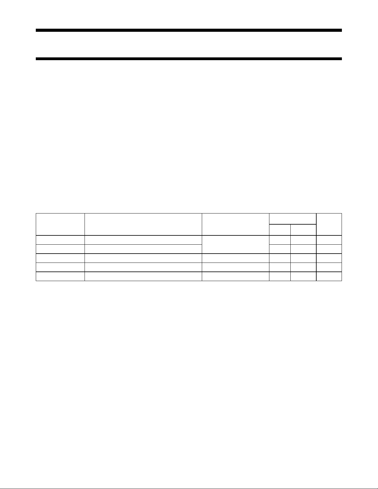
PIN DESCRIPTION
PIN NO. SYMBOL NAME AND FUNCTION
1, 4, 8, 11 Y
7 GND ground (0 V)
2, 3, 9, 10 Z
13, 5, 6, 12 E
14 V
0
0
0
CC
to Y
to Z
to E
3
3
3
independent inputs/outputs
independent inputs/outputs
enable inputs (active HIGH)
positive supply voltage
(a) (b)
Fig.1 Pin configuration. Fig.2 Logic symbol. Fig.3 IEC logic symbol.
December 1990 3
Philips Semiconductors Product specification
Quad bilateral switches 74HC/HCT4016
APPLICATIONS
• Signal gating
• Modulation
• Demodulation
• Chopper
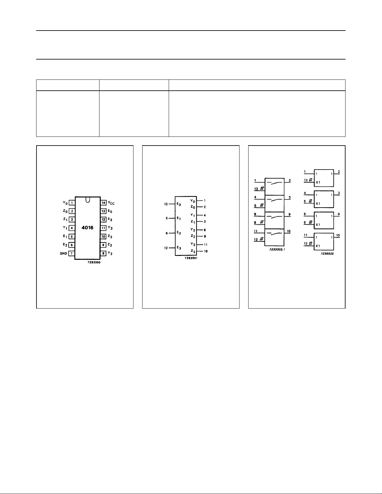
Fig.4 Functional diagram.
FUNCTION TABLE
INPUT
E
n
L
H
Notes
1. H = HIGH voltage level
L = LOW voltage level
CHANNEL
IMPEDANCE
high
low
Fig.5 Schematic diagram (one switch).
December 1990 4

Philips Semiconductors Product specification
Quad bilateral switches 74HC/HCT4016
RATINGS
Limiting values in accordance with the Absolute Maximum System (IEC 134)
Voltages are referenced to GND (ground = 0 V)
SYMBOL PARAMETER MIN. MAX. UNIT CONDITIONS
V
CC
±I
IK
±I
SK
±I
S
±I
; ±I
CC
T
stg
P
tot
P
S
DC supply voltage −0.5 +11.0 V
DC digital input diode current 20 mA for VI<−0.5 V or VI> VCC+ 0.5 V
DC switch diode current 20 mA for VS<−0.5 V or VS> VCC+ 0.5 V
DC switch current 25 mA for −0.5 V < VS< VCC+ 0.5 V
DC VCCor GND current 50 mA
GND
storage temperature range −65 +150 °C
power dissipation per package for temperature range: −40 to +125 °C
74HC/HCT
plastic DIL 750 mW above +70 °C: derate linearly with 12 mW/K
plastic mini-pack (SO) 500 mW above +70 °C: derate linearly with 8 mW/K
power dissipation per switch 100 mW
RECOMMENDED OPERATING CONDITIONS
SYMBOL PARAMETER
V
V
V
T
T
t
r,tf
CC
I
S
amb
amb
DC supply voltage 2.0 5.0 10.0 4.5 5.0 5.5 V
DC input voltage range GND V
DC switch voltage range GND V
operating ambient temperature range −40 +85 −40 +85 °C
operating ambient temperature range −40 +125 −40 +125 °C
input rise and fall times 6.0 500
74HC 74HCT
min. typ. max. min. typ. max.
GND V
CC
GND V
CC
CC
CC
1000 V
6.0 500 ns VCC= 4.5 V
400
250
UNIT CONDITIONS
V
V
see DC and AC
CHARACTERISTICS
= 2.0 V
CC
VCC= 6.0 V
VCC= 10.0 V
December 1990 5
 Loading...