

Philips 74hc hct356 DATASHEETS

INTEGRATED CIRCUITS
DATA SH EET
For a complete data sheet, please also download:
•The IC06 74HC/HCT/HCU/HCMOS Logic Family Specifications
•The IC06 74HC/HCT/HCU/HCMOS Logic Package Information
•The IC06 74HC/HCT/HCU/HCMOS Logic Package Outlines
74HC/HCT356
8-input multiplexer/register; 3-state
Product specification
File under Integrated Circuits, IC06
December 1990
Philips Semiconductors Product specification
8-input multiplexer/register; 3-state 74HC/HCT356
FEATURES
• Non-transparent data latches
• Transparent address latch
• Easily expanding
• Complementary outputs
• Output capability: bus driver
• ICC category: MSI
(LSTTL). They are specified in compliance with JEDEC
standard no. 7A.
The 74HC/HCT356 data selectors/multiplexers contain full
on-chip binary decoding, to select one-of-eight data
sources. The data select address is stored in transparent
latches that are enabled by a LOW on the latch enable
input
LE.
Data on the 8 input lines (D0 to D7) is clocked into a
edge-triggered data register by a LOW-to-HIGH transition
GENERAL DESCRIPTION
The 74HC/HCT356 are high-speed Si-gate CMOS devices
and are pin compatible with low power Schottky TTL
of the clock (CP).
When the output enable input OE1= HIGH, OE2= HIGH
or OE3= LOW, the outputs go to the high impedance
OFF-state.
Operation of these output enable inputs does not affect the
state of the latches and register.
QUICK REFERENCE DATA
GND = 0 V; T
=25°C; tr=tf= 6 ns
amb
SYMBOL PARAMETER CONDITIONS
t
PHL/ tPLH
C
I
C
PD
propagation delay CL= 15 pF; VCC=5 V
,LE to Y, Y2425ns
S
n
CP to Y,
Y2022ns
input capacitance 3.5 3.5 pF
power dissipation capacitance per package notes 1 and 2 123 125 pF
TYPICAL
UNIT
HC HCT
Notes
1. C
is used to determine the dynamic power dissipation (PD in µW):
PD
PD=CPD× V
2
× fi+ ∑ (CL× V
CC
2
× fo) where:
CC
fi= input frequency in MHz
fo= output frequency in MHz
∑ (CL× V
2
× fo) = sum of outputs
CC
CL= output load capacitance in pF
VCC= supply voltage in V
2. For HC the condition is VI= GND to V
CC
For HCT the condition is VI= GND to VCC− 1.5 V
ORDERING INFORMATION
“74HC/HCT/HCU/HCMOS Logic Package Information”
See
.
December 1990 2
Philips Semiconductors Product specification
8-input multiplexer/register; 3-state 74HC/HCT356
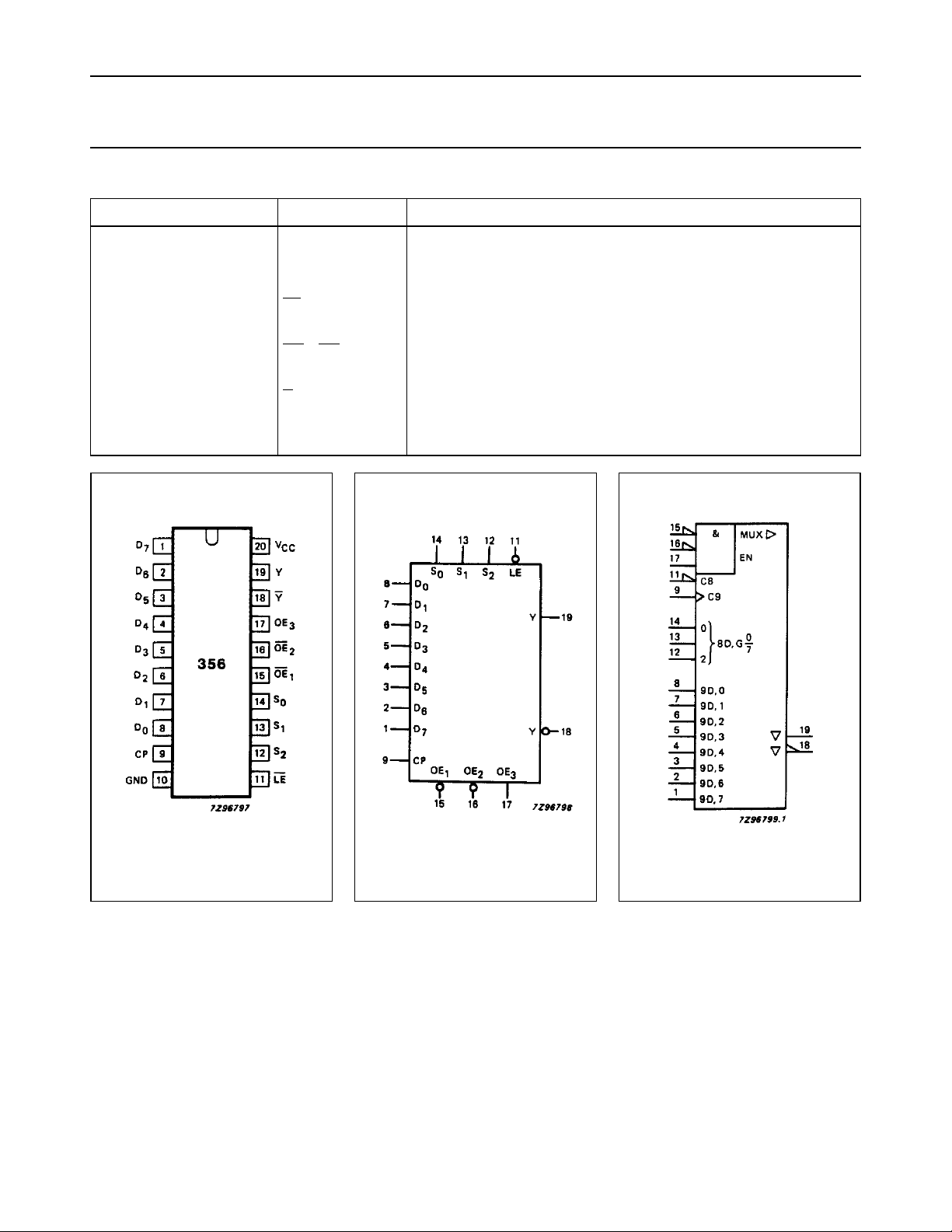
PIN DESCRIPTION
PIN NO. SYMBOL NAME AND FUNCTION
8, 7, 6, 5, 4, 3, 2, 1 D
9 CP clock input data (LOW-to-HIGH, edge-triggered)
10 GND ground (0 V)
11
14, 13, 12 S
15, 16
17 OE
18
19 Y 3-state multiplexer output (active HIGH)
20 V
to D
0
7
data inputs
LE address latch enable input (active LOW)
, S1, S
0
OE1, OE
3
2
2
select inputs
output enable inputs (active LOW)
output enable input (active HIGH)
Y 3-state multiplexer output (active LOW)
CC
positive supply voltage
Fig.1 Pin configuration. Fig.2 Logic symbol. Fig.3 IEC logic symbol.
December 1990 3
Philips Semiconductors Product specification
8-input multiplexer/register; 3-state 74HC/HCT356
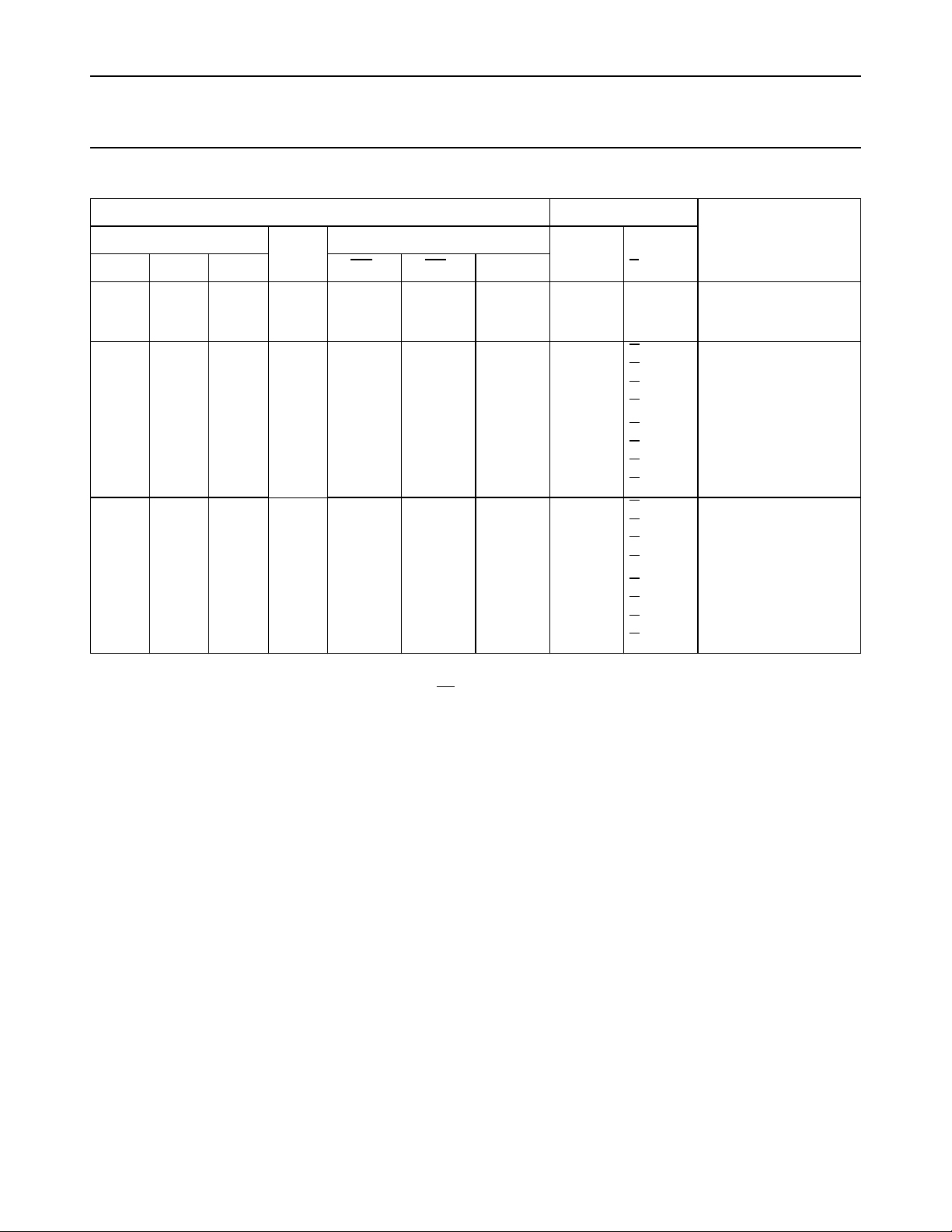
FUNCTION TABLE
INPUTS OUTPUTS
(1)
OUTPUT ENABLE
DESCRIPTIONADDRESS
2
X
X
X
L
L
L
L
H
H
H
H
L
L
L
L
H
H
H
H
S
1
X
X
X
L
L
H
H
L
L
H
H
L
L
H
H
L
L
H
H
X
X
X
L
H
L
H
L
H
L
H
L
H
L
H
L
H
L
H
CP
S
0
X
X
X
↑
↑
↑
↑
↑
↑
↑
↑
(2)
(2)
(2)
(2)
(2)
(2)
(2)
(2)
OE
1
H
X
X
L
L
L
L
L
L
L
L
L
L
L
L
L
L
L
L
OE
2
X
H
X
L
L
L
L
L
L
L
L
L
L
L
L
L
L
L
L
OE
X
X
L
H
H
H
H
H
H
H
H
H
H
H
H
H
H
H
H
Y YS
3
Z
Z
Z
D
0n
D
1n
D
2n
D
3n
D
4n
D
5n
D
6n
D
7n
D
0p
D
1p
D
2p
D
3p
D
4p
D
5p
D
6p
D
7p
Z
Z
Z
D
0n
D
1n
D
2n
D
3n
D
4n
D
5n
D
6n
D
7n
D
0p
D
1p
D
2p
D
3p
D
4p
D
5p
D
6p
D
7p
outputs in
high impedance
OFF-state
data is clocked
into latch
outputs do not
change states
Notes
1. This column shows the input address set-up with
LE = LOW (address latch is transparent).
2. CP is HIGH, LOW or ↓.
3. D0n to D7n= data present at inputs D0 to D7 when the data latch clock made the transition from LOW-to-HIGH
D0p to D7p= data previously latched into the data latch by the LOW-to-HIGH transition of the data latch clock
H = HIGH voltage level
L = LOW voltage level
X = don’t care
↑ = LOW-to-HIGH CP transition
↓ = HIGH-to-LOW CP transition
Z = high impedance OFF-state
December 1990 4
 Loading...