

Philips 74hc hct299 DATASHEETS
INTEGRATED CIRCUITS
DATA SH EET
For a complete data sheet, please also download:
•The IC06 74HC/HCT/HCU/HCMOS Logic Family Specifications
•The IC06 74HC/HCT/HCU/HCMOS Logic Package Information
•The IC06 74HC/HCT/HCU/HCMOS Logic Package Outlines
74HC/HCT299
8-bit universal shift register; 3-state
Product specification
File under Integrated Circuits, IC06
December 1990
Philips Semiconductors Product specification
8-bit universal shift register; 3-state 74HC/HCT299
FEATURES
• Multiplexed inputs/outputs provide improved bit density
• Four operating modes:
– shift left
– shift right
– hold (store)
– load data
• Operates with output enable or at high-impedance
OFF-state (Z)
• 3-state outputs drive bus lines directly
• Can be cascaded for n-bits word length
• Output capability: bus driver (parallel I/Os),
standard (serial outputs)
• ICC category: MSI
GENERAL DESCRIPTION
The 74HC/HCT299 are high-speed Si-gate CMOS devices
and are pin compatible with low power Schottky TTL
(LSTTL). They are specified in compliance with JEDEC
standard no. 7A.
The 74HC/HCT299 contain eight edge-triggered D-type
flip-flops and the interstage logic necessary to perform
synchronous shift-right, shift-left, parallel load and hold
operations. The type of operation is determined by the
mode select inputs (S
and S1), as shown in the mode
0
select table.
All flip-flop outputs have 3-state buffers to separate these
outputs (I/O0 to I/O7) such, that they can serve as data
inputs in the parallel load mode. The serial outputs (Q0 and
Q7) are used for expansion in serial shifting of longer
words.
A LOW signal on the asynchronous master reset input
(MR) overrides the Sn and clock (CP) inputs and resets the
flip-flops. All other state changes are initiated by the rising
edge of the clock pulse. Inputs can change when the clock
is either state, provided that the recommended set-up and
hold times, relative to the rising edge of CP, are observed.
A HIGH signal on the 3-state output enable inputs (OE1 or
OE2) disables the 3-state buffers and the I/On outputs are
set to the high-impedance OFF-state. In this condition, the
shift, hold, load and reset operations can still occur. The
3-state buffers are also disabled by HIGH signals on both
S0 and S1, when in preparation for a parallel load
operation.
QUICK REFERENCE DATA
GND = 0 V; T
=25°C; tr=tf= 6 ns
amb
SYMBOL PARAMETER CONDITIONS
t
PHL/ tPLH
t
PHL
f
max
C
I
C
I/O
C
PD
propagation delay CL= 15 pF; VCC=5 V
CP to Q
CP to I/O
MR to Q0, Q7 or I/O
0
, Q
n
7
n
maximum clock frequency 50 46 MHz
input capacitance 3.5 3.5 pF
input/output capacitance 10 10 pF
power dissipation capacitance per package notes 1 and 2 120 125 pF
Notes
1. CPD is used to determine the dynamic power
dissipation (PD in µW):
PD=CPD× V
2
× fi+ ∑ (CL× V
CC
2
× fo) where:
CC
fi= input frequency in MHz
fo= output frequency in MHz
∑ (CL× V
2
× fo) = sum of outputs
CC
2. For HC the condition is V
For HCT the condition is VI= GND to VCC− 1.5 V
ORDERING INFORMATION
“74HC/HCT/HCU/HCMOS Logic Package
See
Information”
.
CL= output load capacitance in pF
VCC= supply voltage in V
TYPICAL
HC HCT
20 19 ns
20 19 ns
20 23 ns
= GND to V
I
CC
UNIT
December 1990 2
Philips Semiconductors Product specification
8-bit universal shift register; 3-state 74HC/HCT299
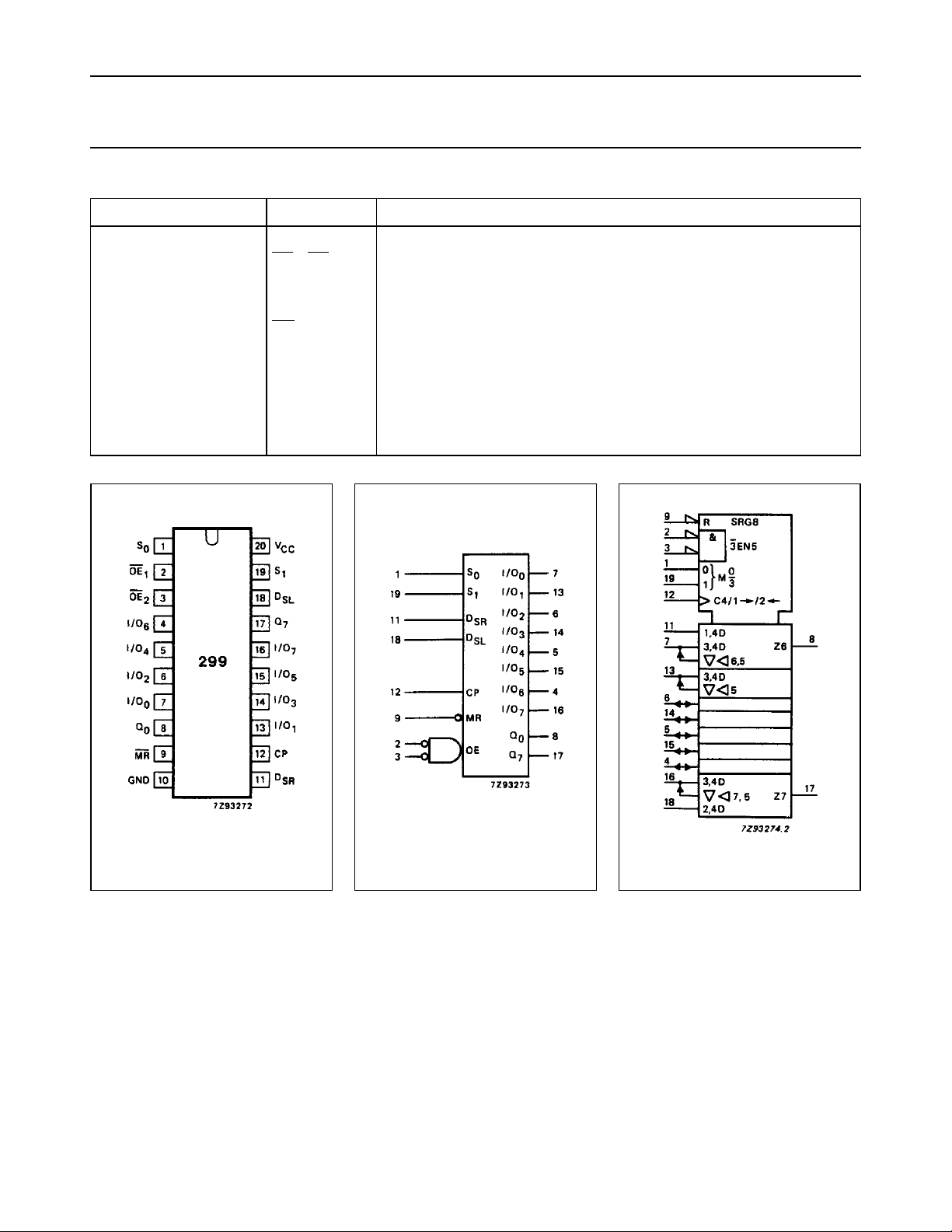
PIN DESCRIPTION
PIN NO. SYMBOL NAME AND FUNCTION
1, 19 S
2, 3
7, 13, 6, 14, 5, 15, 4, 16 I/O
8, 17 Q
9
10 GND ground (0 V)
11 D
12 CP clock input (LOW-to-HIGH, edge-triggered)
18 D
20 V
, S
0
1
OE1, OE
to I/O
0
, Q
0
7
2
mode select inputs
3-state output enable inputs (active LOW)
parallel data inputs or 3-state parallel outputs (bus driver)
7
serial outputs (standard output)
MR asynchronous master reset input (active LOW)
SR
SL
CC
serial data shift-right input
serial data shift-left input
positive supply voltage
Fig.1 Pin configuration. Fig.2 Logic symbol. Fig.3 IEC logic symbol.
December 1990 3
Philips Semiconductors Product specification
8-bit universal shift register; 3-state 74HC/HCT299
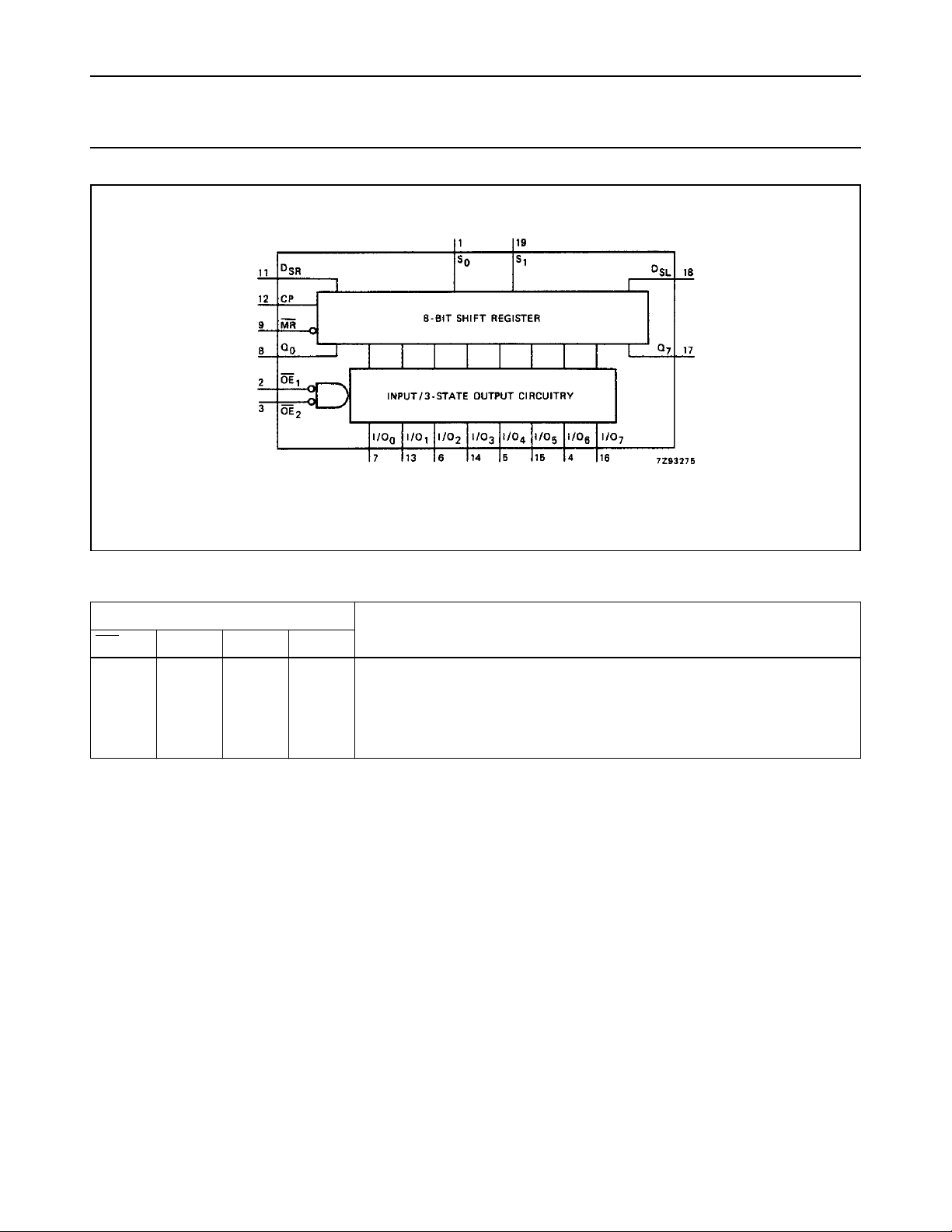
Fig.4 Functional diagram.
MODE SELECT TABLE
INPUTS
MR S
1
S
0
CP
L X X X asynchronous reset; Q
H
H
H
H
H
L
H
L
H
H
L
L
↑
↑
↑
X
parallel load; I/O
n
→ Q
shift right; DSR→ Q0, Q0 → Q1 etc.
shift left; DSL→ Q7, Q7→ Q6 etc.
hold
Notes
1. H = HIGH voltage level
L = LOW voltage level
X = don’t care
↑ = LOW-to-HIGH CP transition
0−Q7
n
RESPONSE
= LOW
December 1990 4
 Loading...