

Philips 74hc hct257 DATASHEETS

INTEGRATED CIRCUITS
DATA SH EET
For a complete data sheet, please also download:
•The IC06 74HC/HCT/HCU/HCMOS Logic Family Specifications
•The IC06 74HC/HCT/HCU/HCMOS Logic Package Information
•The IC06 74HC/HCT/HCU/HCMOS Logic Package Outlines
74HC/HCT257
Quad 2-input multiplexer; 3-state
Product specification
Supersedes data of September 1993
File under Integrated Circuits, IC06
1998 Sep 30
Philips Semiconductors Product specification
Quad 2-input multiplexer; 3-state 74HC/HCT257
FEATURES
• Non-inverting data path
• 3-state outputs interface directly with system bus
• Output capability: bus driver
• ICC category: MSI
The data inputs from source 0 (1I
when input S is LOW and the data inputs from source 1
(1I1 to 4I1) are selected when S is HIGH. Data appears at
the outputs (1Y to 4Y) in true (non-inverting) form from the
selected inputs.
The “257” is the logic implementation of a 4-pole,
2-position switch, where the position of the switch is
GENERAL DESCRIPTION
The 74HC/HCT257 are high-speed Si-gate CMOS devices
and are pin compatible with low power Schottky TTL
(LSTTL). They are specified in compliance with JEDEC
standard no. 7A.
The 74HC/HCT257 have four identical 2-input multiplexers
with 3-state outputs, which select 4 bits of data from two
sources and are controlled by a common data select
input (S).
determined by the logic levels applied to S. The outputs
are forced to a high impedance OFF-state when OE is
HIGH.
The logic equations for the outputs are:
1Y = OE.(1I1.S +1I0.S)
2Y = OE.(2I1.S + 2I0.S)
3Y = OE.(3I1.S + 3I0.S)
4Y = OE.(4I1.S + 4I0.S)
The “257” is identical to the “258” but has non-inverting
(true) outputs.
QUICK REFERENCE DATA
GND = 0 V; T
=25°C; tr=tf= 6 ns
amb
SYMBOL PARAMETER CONDITIONS
t
PHL
/ t
PLH
propagation delay CL= 15 pF; VCC=5 V
nI
, nI1 to nY 11 13 ns
0
S to nY 14 17 ns
C
I
C
PD
input capacitance 3.5 3.5 pF
power dissipation capacitance per multiplexer notes 1 and 2 45 45 pF
to 4I0) are selected
0
TYPICAL
HC HCT
UNIT
Notes
1. C
is used to determine the dynamic power dissipation (PD in µW):
PD
PD=CPD× V
2
× fi+∑(CL× V
CC
2
× fo) where:
CC
fi= input frequency in MHz
fo= output frequency in MHz
∑ (CL× V
2
× fo) = sum of outputs
CC
CL= output load capacitance in pF
VCC= supply voltage in V
2. For HC the condition is VI= GND to V
CC
For HCT the condition is VI= GND to VCC− 1.5 V
1998 Sep 30 2
Philips Semiconductors Product specification
Quad 2-input multiplexer; 3-state 74HC/HCT257
ORDERING INFORMATION
TYPE
NUMBER
74HC257N;
NAME DESCRIPTION VERSION
DIP16 plastic dual in-line package; 16 leads (300 mil); long body SOT38-1
74HCT257N
74HC257D;
SO16 plastic small outline package; 16 leads; body width 3.9 mm SOT109-1
74HCT257D
74HC257DB;
SSOP16 plastic shrink small outline package; 16 leads; body width 5.3 mm SOT338-1
74HCT257DB
74HC257PW;
TSSOP16 plastic thin shrink small outline package; 16 leads; body width 4.4 mm SOT403-1
74HCT257PW
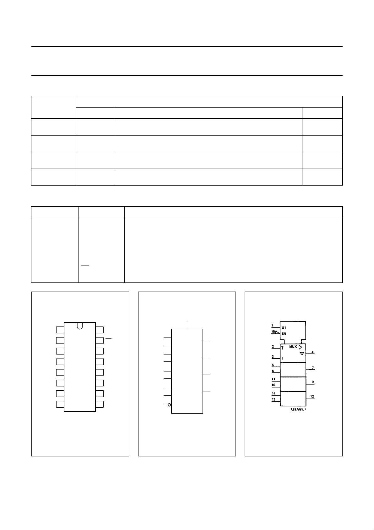
PIN DESCRIPTION
PIN NO. SYMBOL NAME AND FUNCTION
1 S common data select input
2, 5, 11, 14 1I
3, 6, 10, 13 1I
to 4I
0
to 4I
1
0
1
data inputs from source 0
data inputs from source 1
4, 7, 9, 12 1Y to 4Y 3-state multiplexer outputs
8 GND ground (0 V)
15
16 V
OE 3-state output enable input (active LOW)
CC
positive supply voltage
PACKAGE
page
1I
1I
2I
2I
GND
1Y
2Y
S
1
2
0
3
1
4
5
0
6
1
7
8
Fig.1 Pin configuration.
257
MLB311
16
V
CC
15
OE
4I
14
0
4I
13
1
12
4Y
3I
11
0
3I
10
1
9
3Y
page
1I
2
0
1I
3
1
2I
5
0
2I
6
1
3I
11
10
14
13
15
3I
4I
4I
OE
0
1
0
1
Fig.2 Logic symbol.
1998 Sep 30 3
1
S
MGA835
1Y
2Y
3Y
4Y
4
7
9
12
Fig.3 IEC logic symbol.
Philips Semiconductors Product specification
Quad 2-input multiplexer; 3-state 74HC/HCT257
FUNCTION TABLE
INPUTS OUTPUT
OE S nI
2
1I
0
S1
5
3
1I
2I
1
0
11
6
2I
3I
1
0
14
10
3I
1
13
4I
4I
1
0
HXXX Z
LHXL L
SELECTOR
LHXH H
0
nI
1
nY
LLLX L
LLHX H
15
OE
3-STATE MULTIPLEXER OUTPUTS
1Y
4
2Y
7
3Y
12
4Y
9
MGR280
Notes
1. H = HIGH voltage level
L = LOW voltage level
X = don’t care
Z = high impedance OFF-state
Fig.4 Functional diagram.
Fig.5 Logic diagram.
1998 Sep 30 4
 Loading...