

Philips 74hc hct195 DATASHEETS
INTEGRATED CIRCUITS
DATA SH EET
For a complete data sheet, please also download:
•The IC06 74HC/HCT/HCU/HCMOS Logic Family Specifications
•The IC06 74HC/HCT/HCU/HCMOS Logic Package Information
•The IC06 74HC/HCT/HCU/HCMOS Logic Package Outlines
74HC/HCT195
4-bit parallel access shift register
Product specification
File under Integrated Circuits, IC06
December 1990
Philips Semiconductors Product specification
4-bit parallel access shift register 74HC/HCT195
FEATURES
• Asynchronous master reset
• J, K, (D) inputs to the first stage
• Fully synchronous serial or parallel data transfer
• Shift right and parallel load capability
• Complement output from the last stage
• Output capability: standard
• ICC category: MSI
GENERAL DESCRIPTION
The 74HC/HCT195 are high-speed Si-gate CMOS devices
and are pin compatible with low power Schottky TTL
(LSTTL). They are specified in compliance with JEDEC
standard no. 7A.
The 74HC/HCT195 performs serial, parallel,
serial-to-parallel or parallel-to-serial data transfer at very
high speeds. The “195” operates on two primary modes:
shift right (Q
) and parallel load, which are controlled
o→Q1
QUICK REFERENCE DATA
GND = 0 V; T
= 25 °C; tr= tf= 6 ns
amb
by the state of the parallel load enable (PE) input. Serial
data enters the first flip-flop (Q0) via the J and K inputs
when the PE input is HIGH and shifted one bit in the
direction Q0→ Q1→ Q2→ Q3following each
LOW-to-HIGH clock transition. The J and K inputs provide
the flexibility of the JK type input for special applications
and by tying the pins together, the simple D-type input for
general applications. The “195” appears as four common
clocked D flip-flops when the PE input is LOW.
After the LOW-to-HIGH clock transition, data on the
parallel inputs (D0to D3) is transferred to the respective
Q0to Q3outputs. Shift left operation (Q3→ Q2) can be
achieved by tying the Qnoutputs to the D
inputs and
n-1
holding the PE input LOW.
All parallel and serial data transfers are synchronous,
occurring after each LOW-to-HIGH clock transition.
There is no restriction on the activity of the J, K, Dnand
PE inputs for logic operation other than the set-up and
hold time requirements. A LOW on the asynchronous
master reset (MR) input sets all Q outputs LOW,
independent of any other input condition.
SYMBOL PARAMETER CONDITIONS
t
PHL
f
max
C
C
I
PD
/ t
PLH
propagation delay CP to Q
n
CL= 15 pF; VCC= 5 V 15 15 ns
maximum clock frequency 57 57 MHz
input capacitance 3.5 3.5 pF
power dissipation capacitance per package notes 1 and 2 105 105 pF
Notes
1. C
is used to determine the dynamic power dissipation (PDin µW):
PD
PD= CPD× V
2
× fi+∑(CL× V
CC
2
× fo) where:
CC
fi= input frequency in MHz
fo= output frequency in MHz
∑ (CL× V
2
× fo) = sum of outputs
CC
CL= output load capacitance in pF
VCC= supply voltage in V
2. For HC the condition is VI= GND to V
CC
For HCT the condition is VI= GND to VCC− 1,5 V
ORDERING INFORMATION
See
“74HC/HCT/HCU/HCMOS Logic Package Information”
.
TYPICAL
UNIT
HC HCT
December 1990 2
Philips Semiconductors Product specification
4-bit parallel access shift register 74HC/HCT195
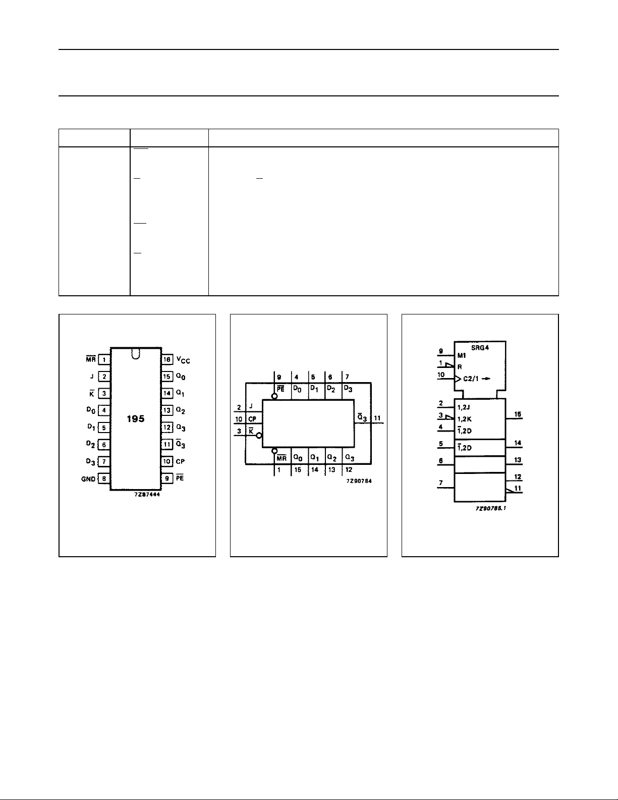
PIN DESCRIPTION
PIN NO. SYMBOL NAME AND FUNCTION
1
2 J first stage J-input (active HIGH)
3
4, 5, 6, 7 D
8 GND ground (0 V)
9
10 CP clock input (LOW-to-HIGH edge-triggered)
11
15, 14, 13, 12 Q
16 V
MR master reset input (active LOW)
K first stage K-input (active LOW)
0
to D
3
parallel data inputs
PE parallel enable input (active LOW)
Q
3
to Q
0
3
CC
inverted output from the last stage
parallel outputs
positive supply voltage
Fig.1 Pin configuration. Fig.2 Logic symbol. Fig.3 IEC logic symbol.
December 1990 3
 Loading...