

Philips 74hc hct194 DATASHEETS

INTEGRATED CIRCUITS
DATA SH EET
For a complete data sheet, please also download:
•The IC06 74HC/HCT/HCU/HCMOS Logic Family Specifications
•The IC06 74HC/HCT/HCU/HCMOS Logic Package Information
•The IC06 74HC/HCT/HCU/HCMOS Logic Package Outlines
74HC/HCT194
4-bit bidirectional universal shift
register
Product specification
File under Integrated Circuits, IC06
December 1990
Philips Semiconductors Product specification
4-bit bidirectional universal shift register 74HC/HCT194
FEATURES
• Shift-left and shift-right capability
• Synchronous parallel and serial data transfer
• Easily expanded for both serial and parallel operation
• Asynchronous master reset
• Hold (“do nothing”) mode
• Output capability: standard
• ICC category: MSI
GENERAL DESCRIPTION
The 74HC/HCT194 are high-speed Si-gate CMOS devices
and are pin compatible with low power Schottky TTL
(LSTTL). They are specified in compliance with JEDEC
standard no. 7A.
The functional characteristics of the 74HC/HCT194 4-bit
bidirectional universal shift registers are indicated in the
logic diagram and function table. The registers are fully
synchronous.
The “194” design has special features which increase the
range of application. The synchronous operation of the
device is determined by the mode select inputs (S
, S1).
0
As shown in the mode select table, data can be entered
and shifted from left to right (Q0→ Q1→ Q2, etc.) or, right
to left (Q3→ Q2→ Q1, etc.) or parallel data can be
entered, loading all 4 bits of the register simultaneously.
When both S0 and S1 are LOW, existing data is retained in
a hold (“do nothing”) mode. The first and last stages
provide D-type serial data inputs (DSR, DSL) to allow
multistage shift right or shift left data transfers without
interfering with parallel load operation.
Mode select and data inputs are edge-triggered,
responding only to the LOW-to-HIGH transition of the
clock (CP). Therefore, the only timing restriction is that the
mode control and selected data inputs must be stable one
set-up time prior to the positive transition of the clock
pulse.
The four parallel data inputs (D0 to D3) are D-type inputs.
Data appearing on the D0 to D3 inputs, when S0 and S1 are
HIGH, is transferred to the Q0 to Q3 outputs respectively,
following the next LOW-to-HIGH transition of the clock.
When LOW, the asynchronous master reset (MR)
overrides all other input conditions and forces the Q
outputs LOW.
The “194” is similar in operation to the “195” universal shift
register, with added features of shift-left without external
connections and hold (“do nothing”) modes of operation.
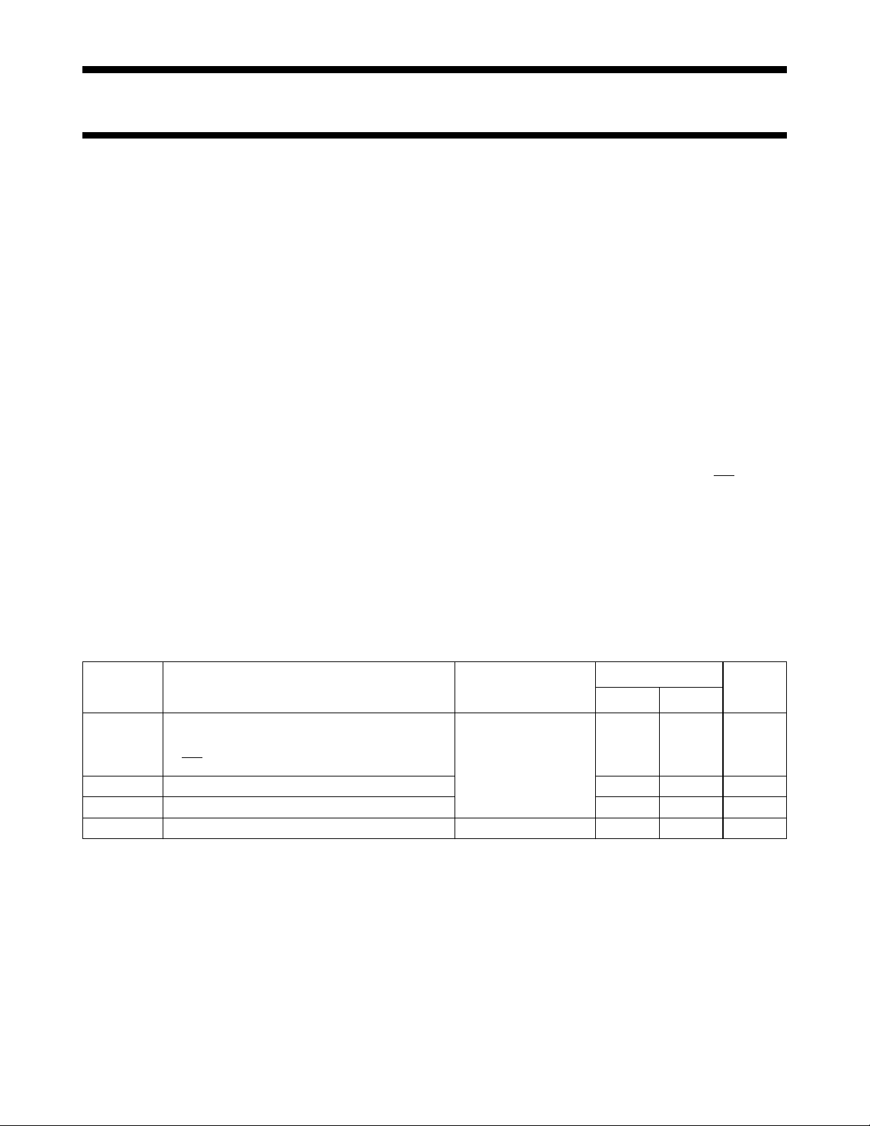
QUICK REFERENCE DATA
GND = 0 V; T
=25°C; tr=tf= 6 ns
amb
SYMBOL PARAMETER CONDITIONS
HC HCT
t
PHL
t
PHL
f
max
C
C
I
PD
/ t
PLH
propagation delay CL= 15 pF; VCC=5 V
CP to Q
MR to Q
n
n
14 15 ns
11 15 ns
maximum clock frequency 102 77 MHz
input capacitance 3.5 3.5 pF
power dissipation capacitance per package notes 1 and 2 40 40 pF
Notes
1. C
is used to determine the dynamic power dissipation (PD in µW):
PD
PD=CPD× V
2
× fi+∑(CL× V
CC
2
× fo) where:
CC
fi= input frequency in MHz
fo= output frequency in MHz
∑ =(CL×V
2
× fo) = sum of outputs
CC
CL= output load capacitance in pF
VCC= supply voltage in V
2. For HC the condition is VI= GND to VCC; for HCT the condition is VI= GND to VCC− 1.5 V
TYPICAL
UNIT
December 1990 2
Philips Semiconductors Product specification
4-bit bidirectional universal shift register 74HC/HCT194
ORDERING INFORMATION
See
“74HC/HCT/HCU/HCMOS Logic Package Information”
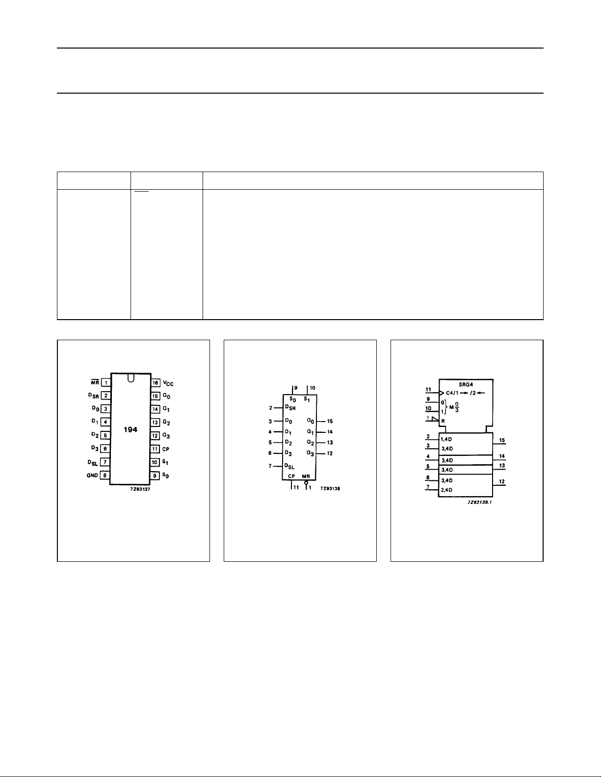
PIN DESCRIPTION
PIN NO. SYMBOL NAME AND FUNCTION
1
2D
3, 4, 5, 6 D
7D
MR asynchronous master reset input (active LOW)
SR
to D
0
SL
3
serial data input (shift right)
parallel data inputs
serial data input (shift left)
8 GND ground (0 V)
9, 10 S
, S
0
1
mode control inputs
11 CP clock input (LOW-to-HIGH edge-triggered)
15, 14, 13, 12 Q
16 V
to Q
0
CC
3
parallel outputs
positive supply voltage
.
Fig.1 Pin configuration. Fig.2 Logic symbol. Fig.3 IEC logic symbol.
December 1990 3
 Loading...