

Philips 74hc hct112 DATASHEETS
INTEGRATED CIRCUITS
DATA SH EET
For a complete data sheet, please also download:
•The IC06 74HC/HCT/HCU/HCMOS Logic Family Specifications
•The IC06 74HC/HCT/HCU/HCMOS Logic Package Information
•The IC06 74HC/HCT/HCU/HCMOS Logic Package Outlines
74HC/HCT112
Dual JK flip-flop with set and reset;
negative-edge trigger
Product specification
Supersedes data of December 1990
File under Integrated Circuits, IC06
1998 Jun 10
Philips Semiconductors Product specification
Dual JK flip-flop with set and reset;
negative-edge trigger
FEATURES
• Asynchronous set and reset
• Output capability: standard
• ICC category: flip-flops
GENERAL DESCRIPTION
The 74HC/HCT112 are high-speed Si-gate CMOS devices
and are pin compatible with low power Schottky TTL
(LSTTL). They are specified in compliance with JEDEC
standard no. 7A.
The 74HC/HCT112 are dual negative-edge triggered
JK-type flip-flops featuring individual nJ, nK, clock (n
CP),
set (nSD) and reset (nRD) inputs.
QUICK REFERENCE DATA
GND = 0 V; T
=25°C; tr=tf= 6 ns
amb
SYMBOL PARAMETER CONDITIONS
t
/ t
PHL
PLH
f
max
C
I
C
PD
propagation delay CL= 15 pF; VCC=5 V
n
CP to nQ, nQ 1719ns
n
S
to nQ, nQ 1515ns
D
n
R
to nQ, nQ 1819ns
D
maximum clock frequency 66 70 MHz
input capacitance 3.5 3.5 pF
power dissipation capacitance per flip-flop notes 1 and 2 27 30 pF
The set and reset inputs, when LOW, set or reset the
outputs as shown in the function table regardless of the
levels at the other inputs.
A HIGH level at the clock (n
nK inputs and data will be accepted. The nJ and nK inputs
control the state changes of the flip-flops as shown in the
function table. The nJ and nK inputs must be stable one
set-up time prior to the HIGH-to-LOW clock transition for
predictable operation.
Output state changes are initiated by the HIGH-to-LOW
transition of nCP.
Schmitt-trigger action in the clock input makes the circuit
highly tolerant to slower clock rise and fall times.
74HC/HCT112
CP) input enables the nJ and
TYPICAL
UNIT
HC HCT
Notes
1. C
is used to determine the dynamic power dissipation (PD in µW):
PD
PD=CPD× V
2
× fi+∑(CL× V
CC
2
× fo) where:
CC
fi= input frequency in MHz
fo= output frequency in MHz
∑ (CL× V
2
× fo) = sum of outputs
CC
CL= output load capacitance in pF
VCC= supply voltage in V
2. For HC the condition is VI= GND to V
CC
For HCT the condition is VI= GND to VCC− 1.5 V
1998 Jun 10 2
Philips Semiconductors Product specification
Dual JK flip-flop with set and reset;
negative-edge trigger
ORDERING INFORMATION
TYPE
NUMBER
74HC112D;
74HCT112D
74HC112DB;
74HCT112DB
74HC112N;
74HCT112N
74HC112PW;
74HCT112PW
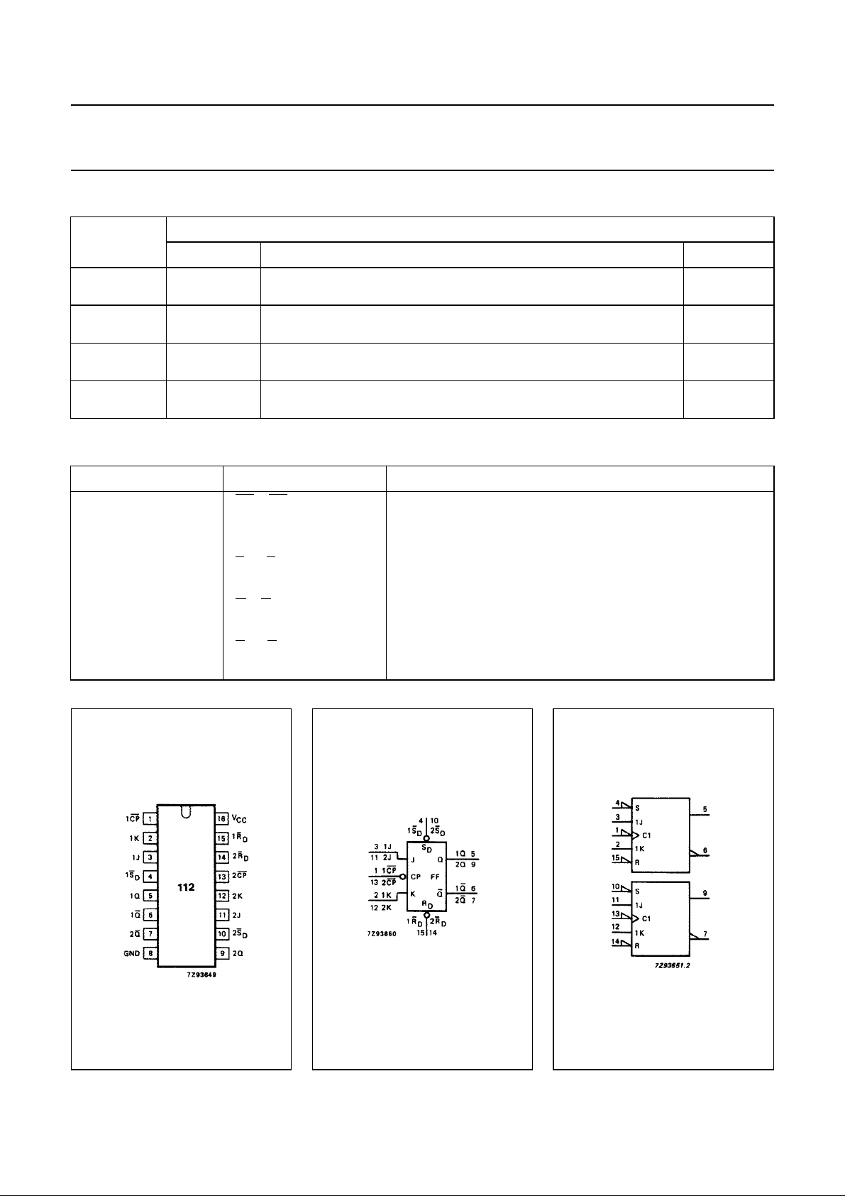
PIN DESCRIPTION
PIN NO. SYMBOL NAME AND FUNCTION
1, 13 1
2, 12 1K, 2K data inputs; flip-flops 1 and 2
3, 11 1J, 2J data inputs; flip-flops 1 and 2
4, 10 1
5, 9 1Q, 2Q true flip-flop outputs
6, 7 1
8 GND ground (0 V)
15, 14 1
16 V
NAME DESCRIPTION VERSION
SO16 plastic small outline package; 16 leads; body width 3.9 mm SOT109-1
SSOP16 plastic shrink small outline package; 16 leads; body width 5.3 mm SOT338-1
DIP16 plastic dual in-line package; 16 leads (300 mil); long body SOT38-1
TSSOP16 plastic thin shrink small outline package; 16 leads; body width 4.4 mm SOT403-1
CP, 2CP clock input (HIGH-to-LOW, edge triggered)
SD, 2S
D
Q, 2Q complement flip-flop outputs
RD, 2R
D
CC
set inputs (active LOW)
reset inputs (active LOW)
positive supply voltage
PACKAGE
74HC/HCT112
Fig.1 Pin configuration. Fig.2 Logic symbol. Fig.3 IEC logic symbol.
1998 Jun 10 3
Philips Semiconductors Product specification
Dual JK flip-flop with set and reset;
negative-edge trigger
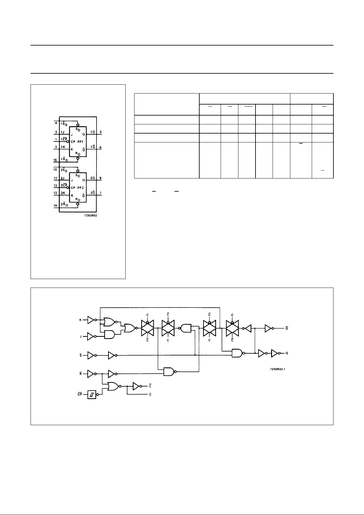
FUNCTION TABLE
OPERATING MODE
asynchronous set L H X X X H L
asynchronous reset H L X X X L H
undetermined L L X X X H L
toggle H H ↓ hh
load “0” (reset) H H ↓ lh L H
load “1” (set) H H ↓ hl H L
hold “no change” H H ↓ ll q
Note
1. If n
SD and nRD simultaneously go from LOW to HIGH, the output states will
be unpredictable.
H = HIGH voltage level
h = HIGH voltage level one set-up time prior to the HIGH-to-LOW CP
transition
L = LOW voltage level
l = LOW voltage level one set-up time prior to the HIGH-to-LOW CP
transition
q = lower case letters indicate the state of the referenced output one set-up
time prior to the HIGH-to-LOW CP transition
Fig.4 Functional diagram.
X = don’t care
↓ = HIGH-to-LOW CP transition
74HC/HCT112
INPUTS OUTPUTS
SDnRDnCP nJ nK nQ nQ
n
qq
q
Fig.5 Logic diagram (one flip-flop).
1998 Jun 10 4

Philips Semiconductors Product specification
Dual JK flip-flop with set and reset;
negative-edge trigger
DC CHARACTERISTICS FOR 74HC
For the DC characteristics see
Output capability: standard
ICCcategory: flip-flops
“74HC/HCT/HCU/HCMOS Logic Family Specifications”
74HC/HCT112
.
1998 Jun 10 5
 Loading...