

Philips 74HCT534U, 74HCT534N, 74HCT534D, 74HC534U, 74HC534N Datasheet
...
DATA SH EET
Product specification
Supersedes data of September 1993
File under Integrated Circuits, IC06
1998 Apr 10
INTEGRATED CIRCUITS
74HC/HCT534
Octal D-type flip-flop; positive
edge-trigger; 3-state; inverting
For a complete data sheet, please also download:
•The IC06 74HC/HCT/HCU/HCMOS Logic Family Specifications
•The IC06 74HC/HCT/HCU/HCMOS Logic Package Information
•The IC06 74HC/HCT/HCU/HCMOS Logic Package Outlines
1998 Apr 10 2
Philips Semiconductors Product specification
Octal D-type flip-flop; positive edge-trigger;
3-state; inverting
74HC/HCT534
FEATURES
• 3-state inverting outputs for bus oriented applications
• 8-bit positive, edge-triggered register
• Common 3-state output enable input
• Output capability: bus driver
• ICC category: MSI.
GENERAL DESCRIPTION
The 74HC/HCT534 are high-speed Si-gate CMOS devices
and are pin compatible with low power Schottky TTL
(LSTTL). They are specified in compliance with JEDEC
standard no. 7A.
The 74HC/HCT534 are octal D-type flip-flops featuring
separate D-type inputs for each flip-flop and inverting
3-state outputs for bus oriented applications. A clock (CP)
and an output enable (
OE) input are common to all
flip-flops.
The 8 flip-flops will store the state of their individual
D-inputs that meet the set-up and hold times requirements
on the LOW-to-HIGH CP transition. When OE is LOW, the
contents of the 8 flip-flops are available at the outputs.
When OE is HIGH, the outputs go to the high impedance
OFF-state. Operation of the OE input does not affect the
state of the flip-flops.
The “534” is functionally identical to the “374”, but has
inverted outputs.
QUICK REFERENCE DATA
GND = 0 V; T
amb
=25°C; tr=tf=6ns
Notes
1. C
PD
is used to determine the dynamic power dissipation (PDin µW):
PD=CPD× V
CC
2
× fi+∑(CL× V
CC
2
× fo) where:
fi= input frequency in MHz.
fo= output frequency in MHz.
∑ (CL× V
CC
2
× fo) = sum of outputs.
CL= output load capacitance in pF.
VCC= supply voltage in V.
2. For HC the condition is VI= GND to VCC; for HCT the condition is VI= GND to VCC− 1.5 V.
ORDERING INFORMATION
SYMBOL PARAMETER CONDITIONS
TYPICAL
UNIT
HC HCT
t
PHL
/ t
PLH
propagation delay CP to Q
n
CL= 15 pF; VCC=5V 12 13 ns
f
max
maximum clock frequency 61 40 MHz
C
I
input capacitance 3.5 3.5 pF
C
PD
power dissipation capacitance per flip-flop notes 1 and 2 19 19 pF
TYPE
NUMBER
PACKAGE
NAME DESCRIPTION VERSION
74HC534 SO20 plastic small outline package; 20 leads; body width 7.5 mm SOT163-1
74HC534 DIP20 plastic dual in-line package; 20 leads (300 mil) SOT146-1
74HCT534 SO20 plastic small outline package; 20 leads; body width 7.5 mm SOT163-1
74HCT534 DIP20 plastic dual in-line package; 20 leads (300 mil) SOT146-1
1998 Apr 10 3
Philips Semiconductors Product specification
Octal D-type flip-flop; positive edge-trigger;
3-state; inverting
74HC/HCT534
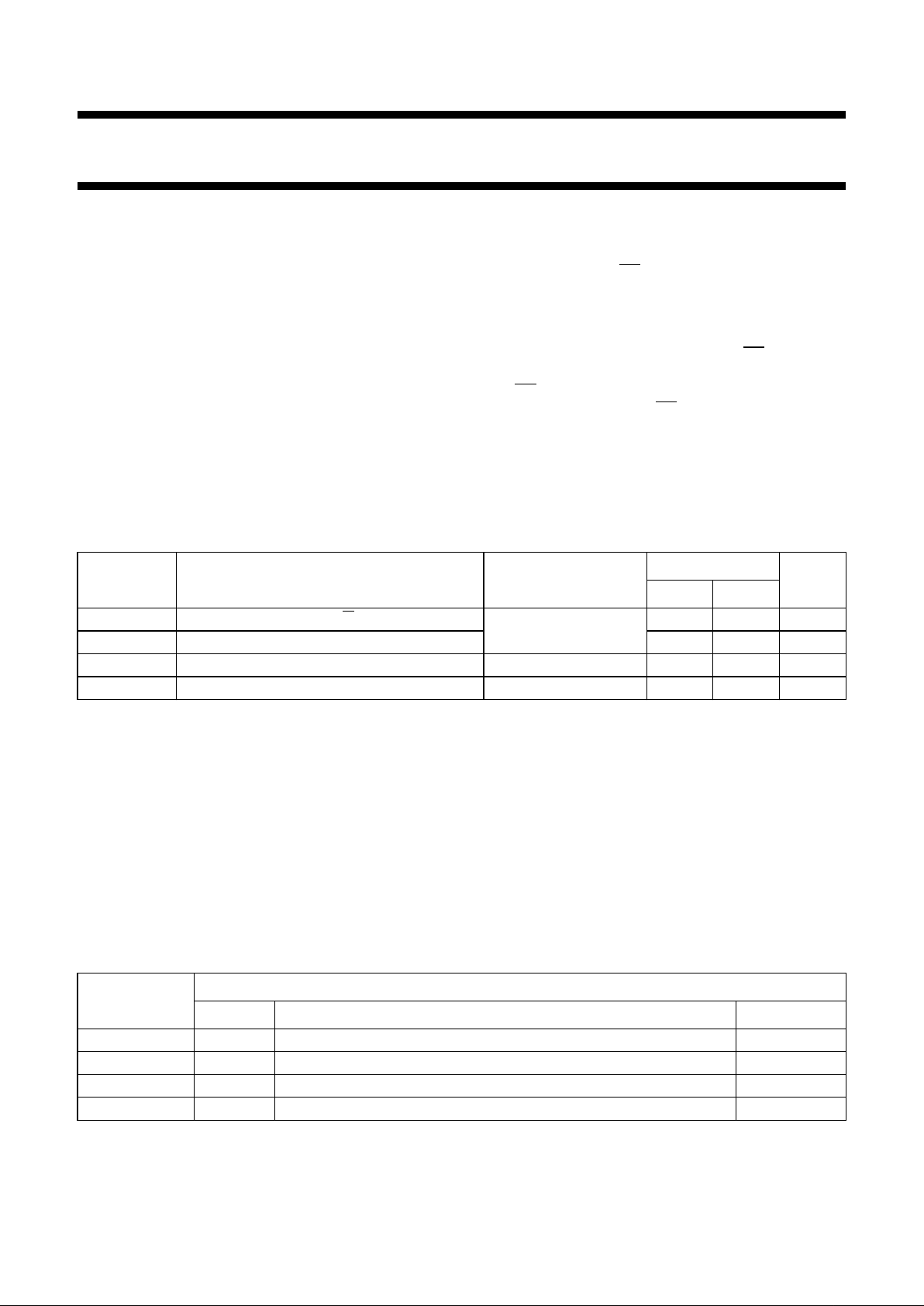
PIN DESCRIPTION
PIN NO. SYMBOL NAME AND FUNCTION
1
OE 3-state output enable input (active LOW)
2, 5, 6, 9, 12, 15, 16, 19
Q0to Q
7
3-state outputs
3, 4, 7, 8, 13, 14, 17, 18 D
0
to D
7
data inputs
10 GND ground (0 V)
11 CP clock input (LOW-to-HIGH, edge-triggered)
20 V
CC
positive supply voltage
Fig.1 Pin configuration.
page
OE
Q
0
D
0
D
1
Q
1
Q
2
D
2
D
3
Q
3
GND
V
CC
Q
7
D
7
D
6
Q
5
D
5
Q
6
D
4
Q
4
CP
1
2
3
4
5
6
7
8
9
10
11
12
20
19
18
17
16
15
14
13
534
MGM954
Fig.2 Logic symbol.
age
MGM955
D
0
D
1
D
2
D
3
D
4
D
5
D
6
D
7
OE
CP
Q
0
Q
1
Q
2
Q
3
Q
4
Q
5
Q
6
Q
7
11
1
19
16
15
12
9
6
5
2
18
17
14
13
8
7
4
3
Fig.3 IEC logic symbol.
page
MGM956
19
16
15
12
9
6
5
11
C1
1
EN
1D
2
18
17
14
13
8
7
4
3
1998 Apr 10 4
Philips Semiconductors Product specification
Octal D-type flip-flop; positive edge-trigger;
3-state; inverting
74HC/HCT534
FUNCTION TABLE
Note
1. H = HIGH voltage level; h = HIGH voltage level one set-up time prior to the LOW-to-HIGH CP transition
L = LOW voltage level; I = LOW voltage level one set-up time prior to the LOW-to-HIGH CP transition
Z = high impedance OFF-state; ↑ = LOW-to-HIGH clock transition.
OPERATING MODES
INPUTS
INTERNAL FLIP-FLOPS
OUTPUTS
OE CP D
n
Q0to Q
7
load and read register L ↑ lL H
L↑hH L
load register and disable outputs H ↑ lL Z
H↑hH Z
Fig.4 Functional diagram.
handbook, halfpage
MGM957
3-STATE
OUTPUTS
Q
0
Q
1
Q
2
Q
3
Q
4
Q
5
Q
6
Q
7
19
16
15
12
9
6
5
2
D
0
D
1
D
2
D
3
D
4
D
5
D
6
D
7
CP
OE
FF1
to
FF8
18
11
1
17
14
13
8
7
4
3
 Loading...