


DATA SH EET
Product specification
File under Integrated Circuits, IC06
December 1990
INTEGRATED CIRCUITS
74HC/HCT4094
8-stage shift-and-store bus register
For a complete data sheet, please also download:
•The IC06 74HC/HCT/HCU/HCMOS Logic Family Specifications
•The IC06 74HC/HCT/HCU/HCMOS Logic Package Information
•The IC06 74HC/HCT/HCU/HCMOS Logic Package Outlines
December 1990 2
Philips Semiconductors Product specification
8-stage shift-and-store bus register 74HC/HCT4094
FEATURES
• Output capability: standard
• ICC category: MSI
GENERAL DESCRIPTION
The 74HC/HCT4094 are high-speed Si-gate CMOS
devices and are pin compatible with the “4094” of the
“4000B” series. They are specified in compliance with
JEDEC standard no. 7A.
The 74HC/HCT4094 are 8-stage serial shift registers
having a storage latch associated with each stage for
strobing data from the serial input (D) to the parallel
buffered 3-state outputs (QP
0
to QP7). The parallel outputs
may be connected directly to common bus lines.
Data is shifted on the positive-going clock (CP) transitions.
The data in each shift register stage is transferred to the
storage register when the strobe input (STR) is HIGH.
Data in the storage register appears at the outputs
whenever the output enable input (OE) signal is HIGH.
Two serial outputs (QS1and QS2) are available for
cascading a number of “4094” devices. Data is available at
QS1on the positive-going clock edges to allow high-speed
operation in cascaded systems in which the clock rise time
is fast. The same serial information is available at QS2on
the next negative-going clock edge and is for cascading
“4094” devices when the clock rise time is slow.
APPLICATIONS
• Serial-to-parallel data conversion
• Remote control holding register
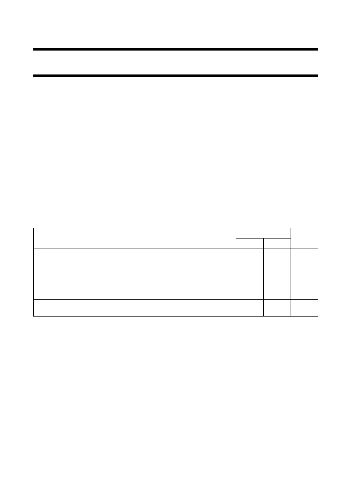
QUICK REFERENCE DATA
GND = 0 V; T
amb
= 25 °C; tr= tf= 6 ns
Notes
1. C
PD
is used to determine the dynamic power dissipation (PDin µW):
PD= CPD× V
CC
2
× fi+∑(CL× V
CC
2
× fo) where:
fi= input frequency in MHz
fo= output frequency in MHz
∑ (CL× V
CC
2
× fo) = sum of outputs
CL= output load capacitance in pF
VCC= supply voltage in V
2. For HC the condition is VI= GND to V
CC
For HCT the condition is VI= GND to VCC− 1.5 V
ORDERING INFORMATION
See
“74HC/HCT/HCU/HCMOS Logic Package Information”
.
SYMBOL PARAMETER CONDITIONS
TYPICAL
UNIT
HC HCT
t
PHL
/ t
PLH
propagation delay CL= 15 pF; VCC= 5 V
CP to QS
1
15 19 ns
CP to QS
2
13 18 ns
CP to QP
n
20 21 ns
STR to QP
n
18 19 ns
f
max
maximum clock frequency 95 86 MHz
C
I
input capacitance 3.5 3.5 pF
C
PD
power dissipation capacitance per package notes 1 and 2 83 92 pF
December 1990 3
Philips Semiconductors Product specification
8-stage shift-and-store bus register 74HC/HCT4094
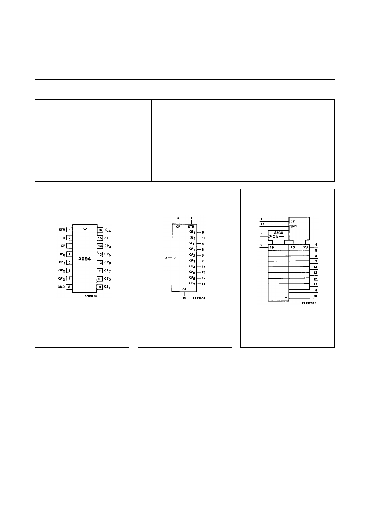
PIN DESCRIPTION
PIN NO. SYMBOL NAME AND FUNCTION
1 STR strobe input
2 D serial input
3 CP clock input
4, 5, 6, 7,14, 13, 12, 11 QP
0
to QP
7
parallel outputs
8 GND ground (0 V)
9, 10 QS
1
,QS
2
serial outputs
15 OE output enable input
16 V
CC
positive supply voltage
Fig.1 Pin configuration. Fig.2 Logic symbol. Fig.3 IEC logic symbol.
 Loading...