

Philips 74HCT259U, 74HCT259PW, 74HCT259N, 74HCT259DB, 74HC259U Datasheet
...
DATA SH EET
Product specification
File under Integrated Circuits, IC06
December 1990
INTEGRATED CIRCUITS
74HC/HCT259
8-bit addressable latch
For a complete data sheet, please also download:
•The IC06 74HC/HCT/HCU/HCMOS Logic Family Specifications
•The IC06 74HC/HCT/HCU/HCMOS Logic Package Information
•The IC06 74HC/HCT/HCU/HCMOS Logic Package Outlines
December 1990 2
Philips Semiconductors Product specification
8-bit addressable latch 74HC/HCT259
FEATURES
• Combines demultiplexer and 8-bit latch
• Serial-to-parallel capability
• Output from each storage bit available
• Random (addressable) data entry
• Easily expandable
• Common reset input
• Useful as a 3-to-8 active HIGH decoder
• Output capability: standard
• ICC category: MSI
GENERAL DESCRIPTION
The 74HC/HCT259 are high-speed Si-gate CMOS devices
and are pin compatible with low power Schottky TTL
(LSTTL). They are specified in compliance with JEDEC
standard no. 7A.
The 74HC/HCT259 are high-speed 8-bit addressable
latches designed for general purpose storage applications
in digital systems. The “259” are multifunctional devices
capable of storing single-line data in eight addressable
latches, and also 3-to-8 decoder and demultiplexer, with
active HIGH outputs (Q
0
to Q7), functions are available.
The “259” also incorporates an active LOW common reset
(MR) for resetting all latches, as well as, an active LOW
enable input (LE).
The “259” has four modes of operation as shown in the
mode select table. In the addressable latch mode, data on
the data line (D) is written into the addressed latch. The
addressed latch will follow the data input with all
non-addressed latches remaining in their previous states.
In the memory mode, all latches remain in their previous
states and are unaffected by the data or address inputs.
In the 3-to-8 decoding or demultiplexing mode, the
addressed output follows the state of the D input with all
other outputs in the LOW state. In the reset mode all
outputs are LOW and unaffected by the address (A0 to A2)
and data (D) input. When operating the “259” as an
addressable latch, changing more than one bit of address
could impose a transient-wrong address. Therefore, this
should only be done while in the memory mode. The mode
select table summarizes the operations of the “259”.
QUICK REFERENCE DATA
GND = 0 V; T
amb
=25°C; tr=tf= 6 ns
Notes
1. C
PD
is used to determine the dynamic power dissipation (PD in µW):
PD=CPD× V
CC
2
× fi+ ∑ (CL× V
CC
2
× fo) where:
fi= input frequency in MHz
fo= output frequency in MHz
∑ (CL× V
CC
2
× fo) = sum of outputs
CL= output load capacitance in pF
VCC= supply voltage in V
2. For HC the condition is VI= GND to V
CC
For HCT the condition is VI= GND to VCC− 1.5 V
SYMBOL PARAMETER CONDITIONS
TYPICAL
UNIT
HC HCT
t
PHL/ tPLH
propagation delay CL= 15 pF; VCC=5 V
D to Q
n
18 20 ns
A
n
, LE to Q
n
17 20 ns
t
PHL
MR to Q
n
15 20 ns
C
I
input capacitance 3.5 3.5 pF
C
PD
power dissipation capacitance per latch notes 1 and 2 19 19 pF
December 1990 3
Philips Semiconductors Product specification
8-bit addressable latch 74HC/HCT259
ORDERING INFORMATION
See
“74HC/HCT/HCU/HCMOS Logic Package Information”
.
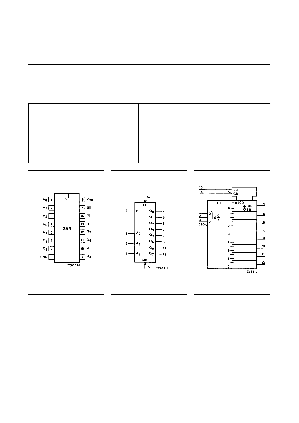
PIN DESCRIPTION
PIN NO. SYMBOL NAME AND FUNCTION
1, 2, 3 A
0
to A
2
address inputs
4, 5, 6, 7, 9 10, 11, 12 Q
0
to Q
7
latch outputs
8 GND ground (0 V)
13 D data input
14
LE latch enable input (active LOW)
15
MR conditional reset input (active LOW)
16 V
CC
positive supply voltage
Fig.1 Pin configuration. Fig.2 Logic symbol. Fig.3 IEC logic symbol.
December 1990 4
Philips Semiconductors Product specification
8-bit addressable latch 74HC/HCT259
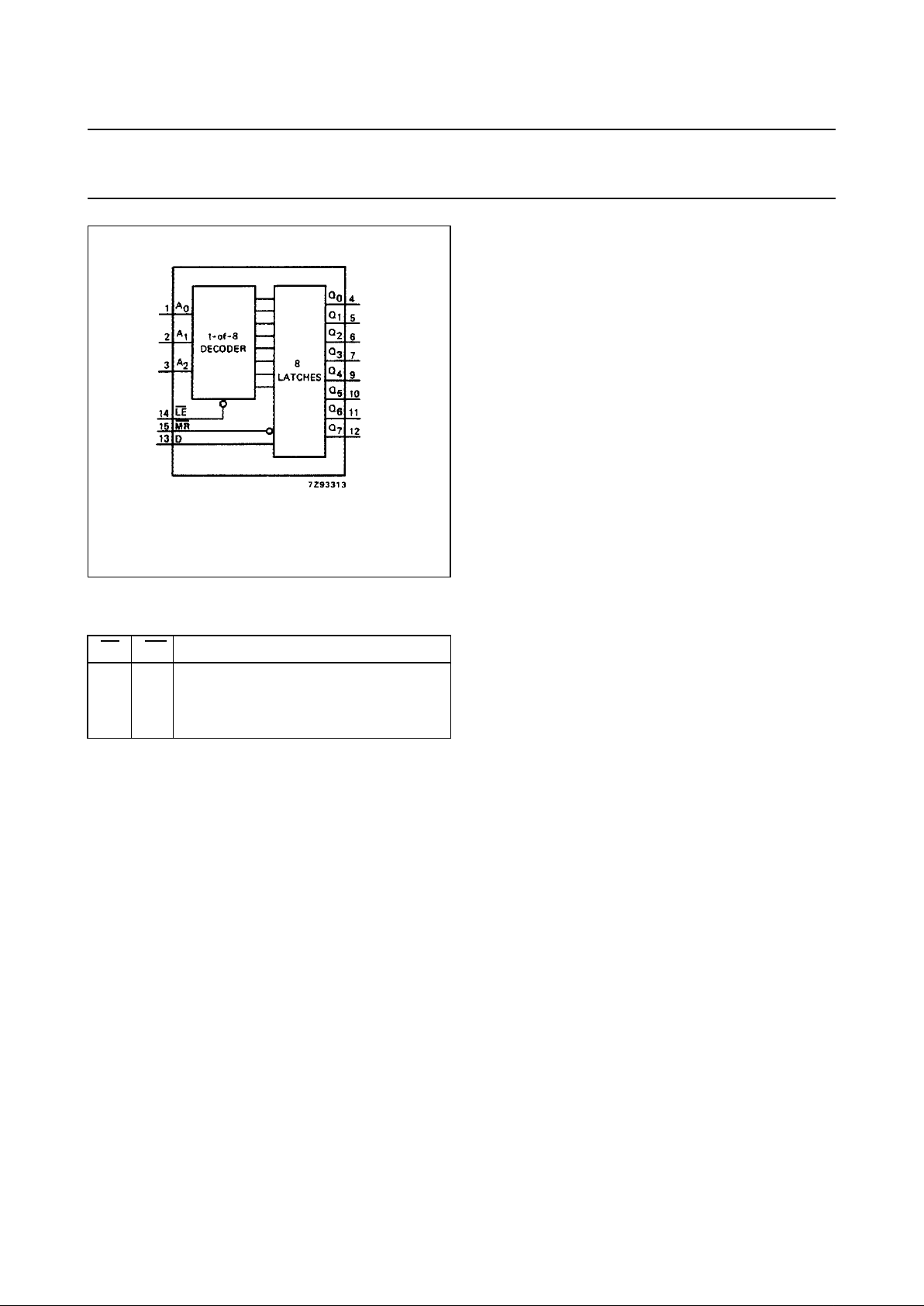
MODE SELECT TABLE
LE MR MODE
L
H
L
H
H
H
L
L
addressable latch
memory
active HIGH 8-channel demultiplexer
reset
Fig.4 Functional diagram.
 Loading...