

Philips 74HCT1G08GW, 74HC1G08GW Datasheet

INTEGRATED CIRCUITS
DATA SH EET
74HC1G08; 74HCT1G08
2-input AND gate
Product specification
File under Integrated Circuits, IC06
1998 Nov 10
Philips Semiconductors Product specification
2-input AND gate
FEATURES
• Wide operating voltage:
2.0 to 6.0 V
• Symmetrical output impedance
• High noise immunity
• Low power dissipation
• Balanced propagation delays
• Very small 5 pins package
• Output capability: standard.
DESCRIPTION
The 74HC1G/HCT1G08 is a
high-speed Si-gate CMOS device.
The 74HC1G/HCT1G08 provides the
2-input AND function. The standard
output currents are
the 74HC/HCT08.
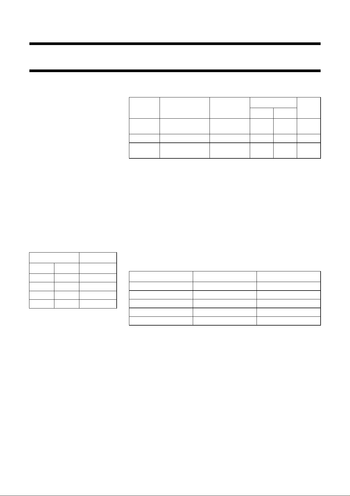
FUNCTION TABLE
See note 1.
1
⁄2 compared to
QUICK REFERENCE DATA
GND = 0 V; T
=25°C; tr=tf≤6.0 ns.
amb
SYMBOL PARAMETER CONDITIONS
t
PHL/tPLH
C
I
C
PD
propagation delay
inA, inB to outY
input capacitance 1.5 1.5 pF
power dissipation
CL= 15 pF;
VCC=5V
notes 1 and 2 19 21 pF
capacitance
Notes
1. C
is used to determine the dynamic power dissipation (PDin µW).
PD
PD=CPD× V
2
× fi+ ∑ (CL× V
CC
2
× fo) where:
CC
fi= input frequency in MHz;
fo= output frequency in MHz;
CL= output load capacitance in pF;
VCC= supply voltage in V;
∑ (CL× V
2. For HC1G the condition is VI= GND to V
2
× fo) = sum of outputs.
CC
CC.
For HCT1G the condition is VI= GND to VCC− 1.5 V.
74HC1G08;
74HCT1G08
TYP.
UNIT
HC1G HCT1G
711ns
INPUTS OUTPUT
inA inB outY
LL L
LH L
HL L
HH H
Note
1. H = HIGH voltage level;
L = LOW voltage level.
PINNING
PIN SYMBOL DESCRIPTION
1 inB data input B
2 inA data input A
3 GND ground (0 V)
4 outY data output
5V
CC
DC supply voltage
1998 Nov 10 2
Philips Semiconductors Product specification
2-input AND gate
74HC1G08;
74HCT1G08
ORDERING AND PACKAGE INFORMATION
OUTSIDE NORTH
AMERICA
74HC1G08GW
74HCT1G08GW 5 SC-88A plastic SOT353 TE
handbook, halfpage
inB
inA
GND
TEMPERATURE
−40 to +125 °C
1
2
08
3
MNA112
RANGE
V
5
outY
4
PINS PACKAGE MATERIAL CODE MARKING
5 SC-88A plastic SOT353 HE
CC
PACKAGES
handbook, halfpage
1
inB
2
inA
outY
MNA113
4
handbook, halfpage
Fig.1 Pin configuration.
1
2
&
4
MNA114
Fig.3 IEC logic symbol.
handbook, halfpage
inB
inA
Fig.2 Logic symbol.
outY
MNA115
Fig.4 Logic diagram.
1998 Nov 10 3
Philips Semiconductors Product specification
2-input AND gate
74HC1G08;
74HCT1G08
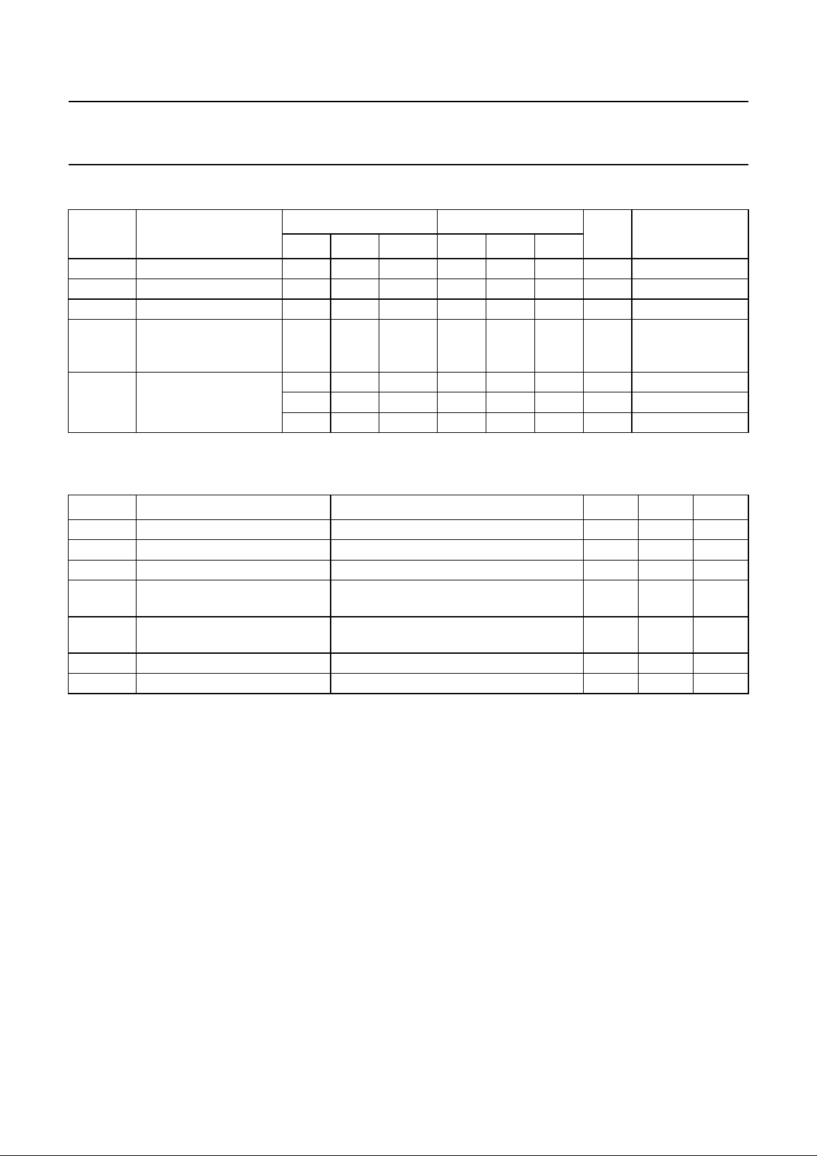
RECOMMENDED OPERATING CONDITIONS
SYMBOL PARAMETER
V
CC
V
I
V
O
T
amb
DC supply voltage 2.0 5.0 6.0 4.5 5.0 5.5 V
input voltage 0 − V
output voltage 0 − V
operating ambient
temperature
t
, t
r
f
input rise and fall times
except for Schmitt
trigger inputs
LIMITING VALUES
In accordance with the Absolute Maximum Rating System (IEC 134); voltages are referenced to GND (ground = 0 V).
SYMBOL PARAMETER CONDITIONS MIN. MAX. UNIT
V
CC
±I
IK
±I
OK
±I
O
DC supply voltage −0.5 +7.0 V
DC input diode current VI< −0.5 V or VI>VCC+ 0.5 V; note 1 − 20 mA
DC output diode current VO< −0.5 V or VO>VCC+ 0.5 V; note 1 − 20 mA
DC output source or sink
current standard outputs
±I
CC
DC VCC or GND current for
types with standard outputs
T
stg
P
D
storage temperature −65 +150 °C
power dissipation per package temperature range: −40 to +125 °C; note 2 − 200 mW
74HC1G04 74HCT1G04
UNIT CONDITIONS
MIN. TYP. MAX. MIN. TYP. MAX.
CC
CC
0 − V
0 − V
CC
CC
V
V
−40 +25 +125 −40 +25 +125 °C see DC and AC
characteristics
per device
−−1000 −−−ns VCC= 2.0 V
−−500 −−500 ns V
−−400 −−−ns V
CC
CC
= 4.5 V
= 6.0 V
−0.5V<VO<VCC+ 0.5 V; note 1 − 12.5 mA
note 1 − 25 mA
Notes
1. The input and output voltage ratings may be exceeded if the input and output current ratings are observed.
2. Above 55 °C the value of P
derates linearly with 2.5 mW/K.
D
1998 Nov 10 4
 Loading...