

Philips 74HCT1G00GW, 74HC1G00GW Datasheet

INTEGRATED CIRCUITS
DATA SH EET
74HC1G00; 74HCT1G00
2-input NAND gate
Product specification
File under Integrated Circuits, IC06
1998 Jul 30
Philips Semiconductors Product specification
2-input NAND gate
FEATURES
• Wide operating voltage:
2.0 to 6.0 V
• Symmetrical output impedance
• High noise immunity
• Low power dissipation
• Balanced propagation delays
• Very small 5 pins package
• Output capability: standard.
DESCRIPTION
The 74HC1G/HCT1G00 is a high
speed Si-gate CMOS device.
The 74HC1G/HCT1G00 provides the
2-input NAND function. The standard
output currents are
the 74HC/HCT00.
FUNCTION TABLE
See note 1.
INPUTS OUTPUT
inA inB outY
LL H
LH H
HL H
HH L
Note
1. H = HIGH voltage level;
L = LOW voltage level.
1
⁄2 compared to
QUICK REFERENCE DATA
GND = 0 V; T
=25°C; tr=tf≤6.0 ns
amb
SYMBOL PARAMETER CONDITIONS
t
PHL/tPLH
propagation
delay
CL=15pF;
VCC=5V
inA, inB to outY
C
I
input
capacitance
C
PD
power
notes 1 and 2 19 21 pF
dissipation
capacitance
Notes
1. C
is used to determine the dynamic power dissipation (PDin µW).
PD
PD=CPD× V
2
× fi+ ∑ (CL× V
CC
2
× fo) where:
CC
fi= input frequency in MHz;
fo= output frequency in MHz;
CL= output load capacitance in pF;
VCC= supply voltage in V;
∑ (CL× V
2. For HC1G the condition is VI= GND to V
2
× fo) = sum of outputs.
CC
CC.
For HCT1G the condition is VI= GND to VCC− 1.5 V.
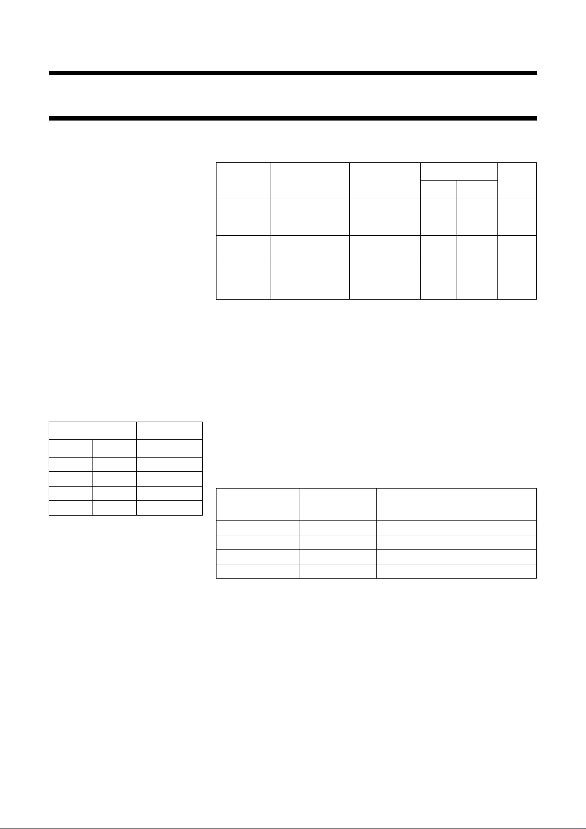
PINNING
PIN SYMBOL DESCRIPTION
1 inB data input B
2 inA data input A
3 GND ground (0 V)
4 outY data output
5V
CC
DC supply voltage
74HC1G00;
74HCT1G00
TYPICAL
UNIT
HC1G HCT1G
710ns
1.5 1.5 pF
1998 Jul 30 2
Philips Semiconductors Product specification
2-input NAND gate 74HC1G00; 74HCT1G00
ORDERING INFORMATION
PACKAGES
OUTSIDE NORTH AMERICA
74HC1G00GW
74HCT1G00GW 5 SC-88A plastic SOT353 TA
TEMPERATURE
RANGE
−40 to +125 °C
PINS PACKAGE MATERIAL CODE MARKING
5 SC-88A plastic SOT353 HA
handbook, halfpage
handbook, halfpage
inB
inA
GND
1
2
3
5
00
4
MNA096
Fig.1 Pin configuration.
1
2
&
MNA098
V
CC
outY
handbook, halfpage
1
inB
2
inA
outY
MNA097
4
Fig.2 Logic symbol.
handbook, halfpage
4
inB
inA
outY
MNA099
Fig.3 IEC logic symbol.
1998 Jul 30 3
Fig.4 Logic diagram.
Philips Semiconductors Product specification
2-input NAND gate 74HC1G00; 74HCT1G00
RECOMMENDED OPERATING CONDITIONS
SYMBOL PARAMETER
UNIT CONDITIONS
MIN. TYP. MAX. MIN. TYP. MAX.
74HC1G 74HCT1G
V
CC
V
I
V
O
T
amb
DC supply voltage 2.0 5.0 6.0 4.5 5.0 5.5 V
input voltage 0 − V
output voltage 0 − V
operating ambient
−40 +25 +125 −40 +25 +125 °C see DC and AC
0 − V
CC
0 − V
CC
CC
CC
temperature range
V
V
characteristics per
device
t
, t
r
f
input rise and fall times
except for
Schmitt-trigger inputs
−−1000 −−− ns VCC= 2.0 V
−−500 −−500 V
−−400 −−− V
CC
CC
= 4.5 V
= 6.0 V
LIMITING VALUES
In accordance with the Absolute Maximum Rating System (IEC 134); voltages are referenced to GND (ground = 0 V);
see note 1 and 2.
SYMBOL PARAMETER CONDITIONS MIN. MAX. UNIT
V
CC
±I
IK
±I
OK
±I
O
±I
CC
DC supply voltage −0.5 +7.0 V
DC input diode current VI<−0.5 or VI> VCC+ 0.5 V − 20 mA
DC output diode current VO<−0.5 or VO> VCC+ 0.5 V − 20 mA
DC output source or sink
current standard outputs
DC VCC or GND current for
−0.5 V < VO< VCC+ 0.5 V
− 12.5 mA
− 25 mA
types with standard outputs
T
stg
P
D
storage temperature range −65 +150 °C
power dissipation per
package 5 pins plastic SC-88A
for temperature range: −40 to +125 °C;
above +55 °C derate linearly with 2.5 mW/K
− 200 mW
Notes
1. Stresses beyond those listed may cause permanent damage to the device. These are stress rating only and
functional operation of the device at these or any other conditions beyond those under ‘recommended operating
conditions’ is not implied. Exposure to absolute maximum rated conditions for extended periods may affect device
reliability.
2. The input and output voltage ratings may be exceeded if the input and output current ratings are observed.
1998 Jul 30 4
 Loading...