

Philips 74HCT174DB, 74HCT174D, 74HCT174PW, 74HCT174N, 74HC174U Datasheet
...
DATA SH EET
Product specification
Supersedes data of September 1993
File under Integrated Circuits, IC06
1998 Jul 08
INTEGRATED CIRCUITS
74HC/HCT174
Hex D-type flip-flop with reset;
positive-edge trigger
For a complete data sheet, please also download:
•The IC06 74HC/HCT/HCU/HCMOS Logic Family Specifications
•The IC06 74HC/HCT/HCU/HCMOS Logic Package Information
•The IC06 74HC/HCT/HCU/HCMOS Logic Package Outlines
1998 Jul 08 2
Philips Semiconductors Product specification
Hex D-type flip-flop with reset; positive-edge trigger 74HC/HCT174
FEATURES
• Six edge-triggered D-type flip-flops
• Asynchronous master reset
• Output capability: standard
• ICC category: MSI
GENERAL DESCRIPTION
The 74HC/HCT174 are high-speed Si-gate CMOS devices
and are pin compatible with low power Schottky TTL
(LSTTL). They are specified in compliance with JEDEC
standard no. 7A.
The 74HC/HCT174 have six edge-triggered D-type
flip-flops with individual D inputs and Q outputs. The
common clock (CP) and master reset (
MR) inputs load and
reset (clear) all flip-flops simultaneously.
The register is fully edge-triggered. The state of each D
input, one set-up time prior to the LOW-to-HIGH clock
transition, is transferred to the corresponding output of the
flip-flop.
A LOW level on the MR input forces all outputs LOW,
independently of clock or data inputs.
The device is useful for applications requiring true outputs
only and clock and master reset inputs that are common to
all storage elements.
QUICK REFERENCE DATA
GND = 0 V; T
amb
=25°C; tr=tf= 6 ns
Notes
1. C
PD
is used to determine the dynamic power dissipation (PD in µW):
PD=CPD× V
CC
2
× fi+∑ (CL× V
CC
2
× fo) where:
fi= input frequency in MHz
fo= output frequency in MHz
∑ (CL× V
CC
2
× fo) = sum of outputs
CL= output load capacitance in pF
VCC= supply voltage in V
2. For HC the condition is VI= GND to V
CC
For HCT the condition is VI= GND to VCC− 1.5 V
SYMBOL PARAMETER CONDITIONS
TYPICAL
UNIT
HC HCT
t
PHL
/ t
PLH
propagation delay CL= 15 pF; VCC=5 V
CP to Q
n
17 18 ns
MR to Q
n
13 17 ns
f
max
maximum clock frequency 99 69 MHz
C
I
input capacitance 3.5 3.5 pF
C
PD
power dissipation
capacitance per flip-flop
notes 1 and 2 17 17 pF
1998 Jul 08 3
Philips Semiconductors Product specification
Hex D-type flip-flop with reset; positive-edge trigger 74HC/HCT174
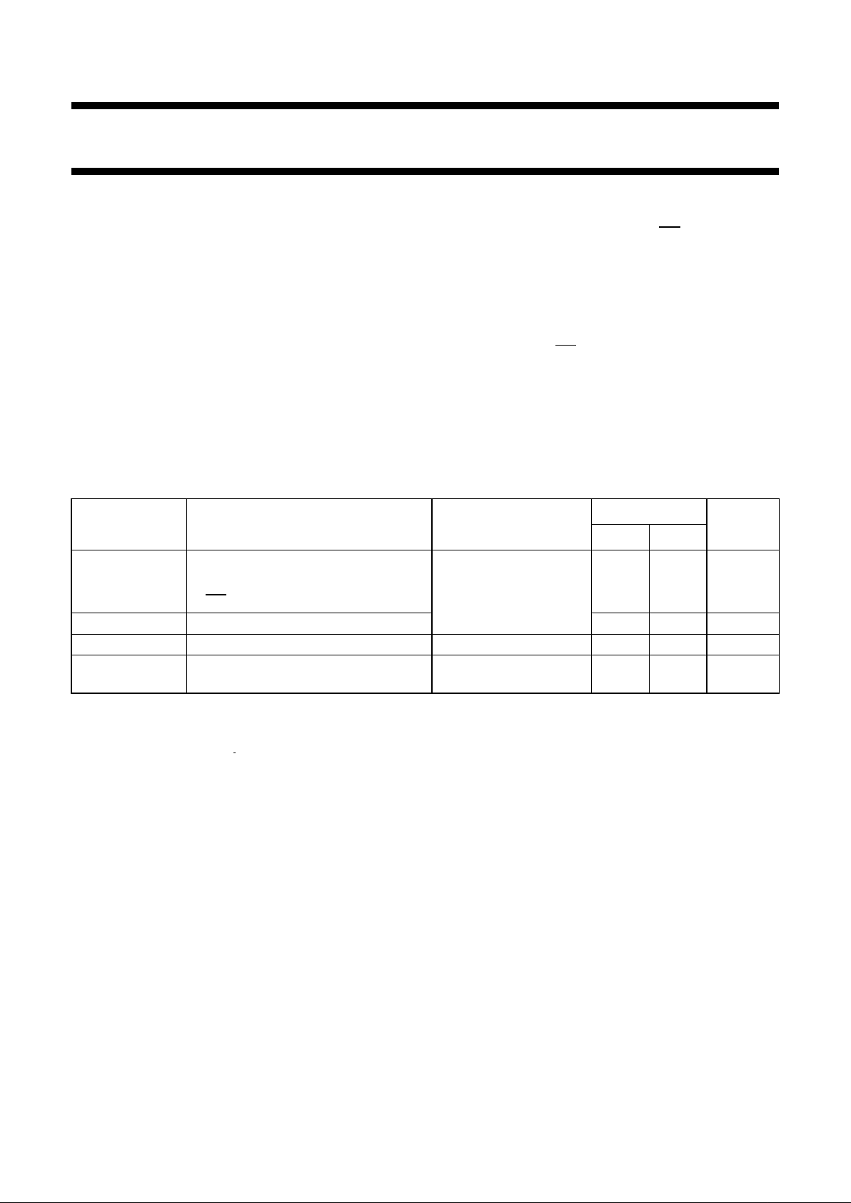
ORDERING INFORMATION
PIN DESCRIPTION
TYPE
NUMBER
PACKAGE
NAME DESCRIPTION VERSION
74HC174N;
74HCT174N
DIP16 plastic dual in-line package; 16 leads (300 mil); long body SOT38-1
74HC174D;
74HCT174D
SO16 plastic small outline package; 16 leads; body width 3.9 mm SOT109-1
74HC174DB;
74HCT174DB
SSOP16 plastic shrink small outline package; 16 leads; body width 5.3 mm SOT338-1
74HC174PW;
74HCT174PW
TSSOP16 plastic thin shrink small outline package; 16 leads; body width 4.4 mm SOT403-1
PIN NO. SYMBOL NAME AND FUNCTION
1
MR asynchronous master reset (active LOW)
2, 5, 7, 10, 12, 15 Q
0
to Q
5
flip-flop outputs
3, 4, 6, 11, 13, 14 D
0
to D
5
data inputs
8 GND ground (0 V)
9 CP clock input (LOW-to-HIGH, edge-triggered)
16 V
CC
positive supply voltage
Fig.1 Pin configuration. Fig.2 Fig.3 IEC logic symbol.
1998 Jul 08 4
Philips Semiconductors Product specification
Hex D-type flip-flop with reset; positive-edge trigger 74HC/HCT174
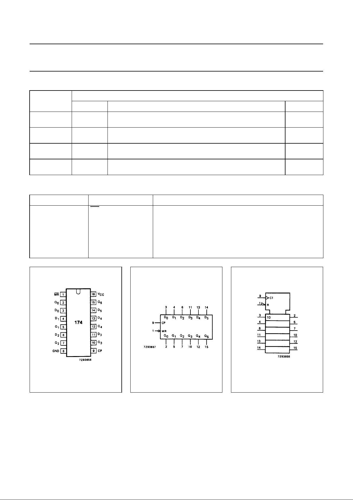
FUNCTION TABLE
Note
1. H = HIGH voltage level
h = HIGH voltage level one set-up time prior to the LOW-to-HIGH CP transition
L = LOW voltage level
I = LOW voltage level one set-up time prior to the LOW-to-HIGH CP transition
X = don’t care
↑= LOW-to-HIGH CP transition
OPERATING MODES
INPUTS OUTPUTS
MR CP D
n
Q
n
reset (clear) L X X L
load “1” H ↑ hH
load “0” H ↑ IL
Fig.4 Functional diagram.
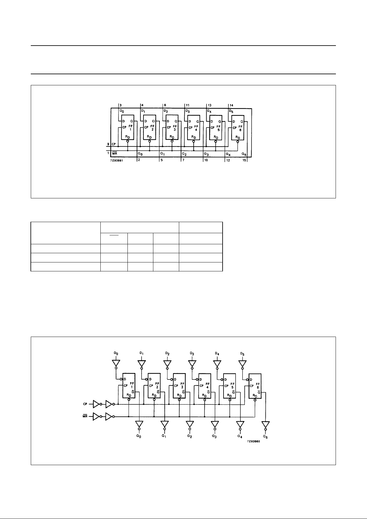
Fig.5 Logic diagram.
 Loading...