

Philips 74HCT166N, 74HCT166DB, 74HCT166D, 74HCT166U, 74HC166U Datasheet
...
DATA SH EET
Product specification
File under Integrated Circuits, IC06
December 1990
INTEGRATED CIRCUITS
74HC/HCT166
8-bit parallel-in/serial-out shift
register
For a complete data sheet, please also download:
•The IC06 74HC/HCT/HCU/HCMOS Logic Family Specifications
•The IC06 74HC/HCT/HCU/HCMOS Logic Package Information
•The IC06 74HC/HCT/HCU/HCMOS Logic Package Outlines
December 1990 2
Philips Semiconductors Product specification
8-bit parallel-in/serial-out shift register 74HC/HCT166
FEATURES
• Synchronous parallel-to-serial applications
• Synchronous serial data input for easy expansion
• Clock enable for “do nothing” mode
• Asynchronous master reset
• For asynchronous parallel data load see “165”
• Output capability: standard
• ICC category: MSI
GENERAL DESCRIPTION
The 74HC/HCT166 are high-speed Si-gate CMOS devices
and are pin compatible with low power Schottky TTL
(LSTTL). They are specified in compliance with JEDEC
standard no. 7A.
The 74HC/HCT166 are 8-bit shift registers which have a
fully synchronous serial or parallel data entry selected by
an active LOW parallel enable (
PE) input. When PE is
LOW one set-up time prior to the LOW-to-HIGH clock
transition, parallel data is entered into the register. When
PE is HIGH, data is entered into the internal bit position Q
0
from serial data input (Ds), and the remaining bits are
shifted one place to the right (Q0→ Q1→ Q2, etc.) with
each positive-going clock transition.
This feature allows parallel-to-serial converter expansion
by tying the Q7 output to the Ds input of the succeeding
stage.
The clock input is a gated-OR structure which allows one
input to be used as an active LOW clock enable (CE) input.
The pin assignment for the CP and CE inputs is arbitrary
and can be reversed for layout convenience. The
LOW-to-HIGH transition of inputCE should only take place
while CP is HIGH for predictable operation. A LOW on the
master reset (MR) input overrides all other inputs and
clears the register asynchronously, forcing all bit positions
to a LOW state.
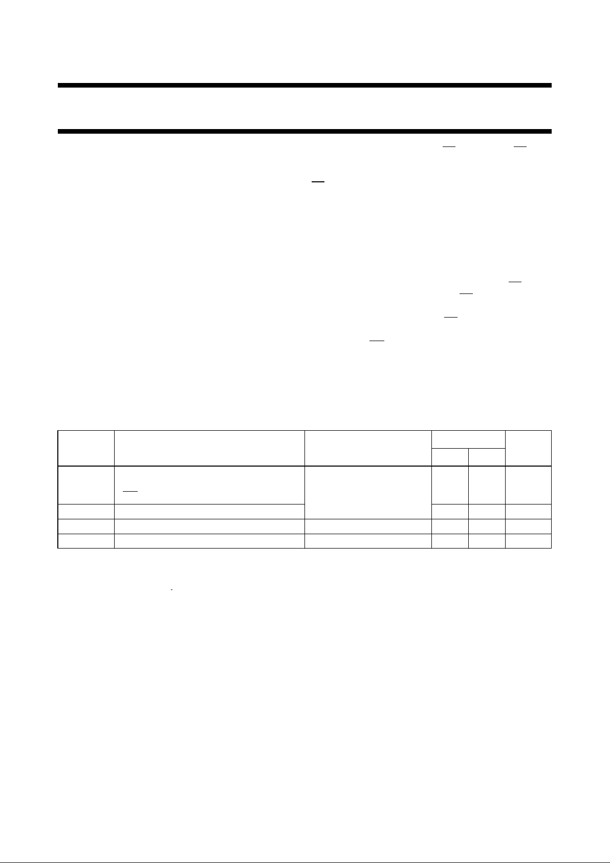
QUICK REFERENCE DATA
GND = 0 V; T
amb
=25°C; tr=tf= 6 ns
Notes
1. C
PD
is used to determine the dynamic power dissipation (PD in µW):
PD=CPD× V
CC
2
× fi+ ∑ (CL× V
CC
2
× fo) where:
fi= input frequency in MHz
fo= output frequency in MHz
∑ (CL× V
CC
2
× fo) = sum of outputs
CL= output load capacitance in pF
VCC= supply voltage in V
2. For HC the condition is VI= GND to V
CC
For HCT the condition is VI= GND to VCC− 1.5 V
ORDERING INFORMATION
See
“74HC/HCT/HCU/HCMOS Logic Package Information”
.
SYMBOL PARAMETER CONDITIONS
TYPICAL
UNIT
HC HCT
t
PHL
/ t
PLH
propagation delay
CP to Q
7
MR to Q
7
CL= 15 pF; VCC=5 V
15
14
20
19
ns
ns
f
max
maximum clock frequency 63 50 MHz
C
I
input capacitance 3.5 3.5 pF
C
PD
power dissipation capacitance per package notes 1 and 2 41 41 pF
December 1990 3
Philips Semiconductors Product specification
8-bit parallel-in/serial-out shift register 74HC/HCT166
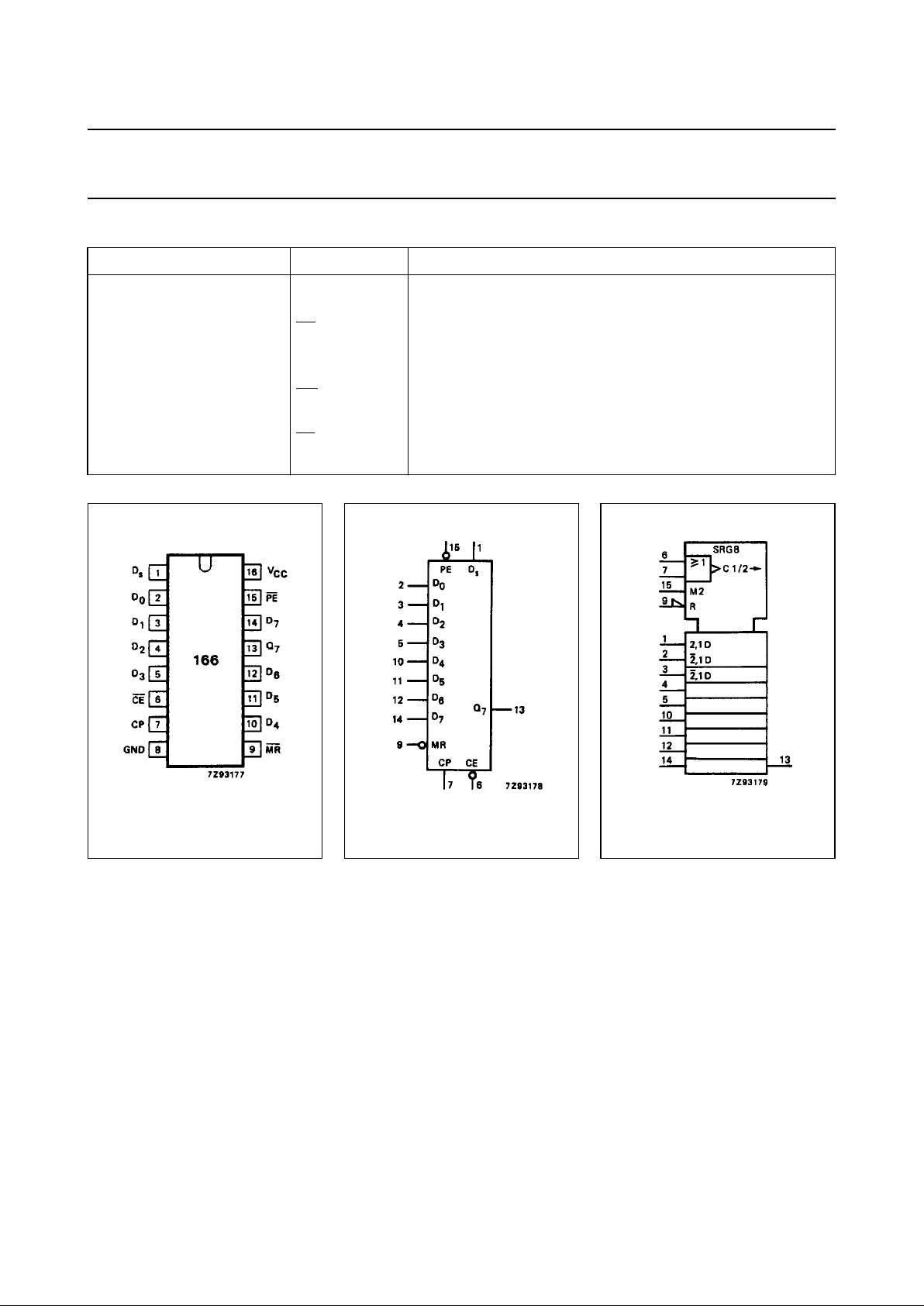
PIN DESCRIPTION
PIN NO. SYMBOL NAME AND FUNCTION
1D
s
serial data input
2, 3, 4, 5, 10, 11, 12, 14 D
0
to D
7
parallel data inputs
6
CE clock enable input (active LOW)
7 CP clock input (LOW-to-HIGH edge-triggered)
8 GND ground (0 V)
9
MR asynchronous master reset (active LOW)
13 Q
7
serial output from the last stage
15
PE parallel enable input (active LOW)
16 V
CC
positive supply voltage
Fig.1 Pin configuration. Fig.2 Logic symbol. Fig.3 IEC logic symbol.
 Loading...