

Philips 74HCT132U, 74HCT132PW, 74HCT132N, 74HCT132D, 74HC132U Datasheet
...
DATA SH EET
Product specification
File under Integrated Circuits, IC06
September 1993
INTEGRATED CIRCUITS
74HC/HCT132
Quad 2-input NAND Schmitt trigger
For a complete data sheet, please also download:
•The IC06 74HC/HCT/HCU/HCMOS Logic Family Specifications
•The IC06 74HC/HCT/HCU/HCMOS Logic Package Information
•The IC06 74HC/HCT/HCU/HCMOS Logic Package Outlines

September 1993 2
Philips Semiconductors Product specification
Quad 2-input NAND Schmitt trigger 74HC/HCT132
FEATURES
• Output capability: standard
• ICC category: SSI
GENERAL DESCRIPTION
The 74HC/HCT132 are high-speed Si-gate CMOS devices and are pin compatible with low power Schottky TTL (LSTTL).
They are specified in compliance with JEDEC standard no. 7A.
The 74HC/HCT132 contain four 2-input NAND gates which accept standard input signals. They are capable of
transforming slowly changing input signals into sharply defined, jitter-free output signals.
The gate switches at different points for positive and negative-going signals. The difference between the positive voltage
V
T+
and the negative voltage VT− is defined as the hysteresis voltage VH.
QUICK REFERENCE DATA
GND = 0 V; T
amb
=25°C; tr=tf= 6 ns
Notes
1. C
PD
is used to determine the dynamic power dissipation (PD in µW):
PD=CPD× V
CC
2
× fi+∑(CL× V
CC
2
× fo) where:
fi= input frequency in MHz
fo= output frequency in MHz
∑ (CL× V
CC
2
× fo) = sum of outputs
CL= output load capacitance in pF
VCC= supply voltage in V
2. For HC the condition is VI= GND to V
CC
For HCT the condition is VI= GND to VCC− 1.5 V
ORDERING INFORMATION
See
“74HC/HCT/HCU/HCMOS Logic Package Information”
.
SYMBOL PARAMETER CONDITIONS
TYPICAL
UNIT
HC HCT
t
PHL
/ t
PLH
propagation delay nA, nB to nY CL= 15 pF; VCC=5 V 11 17 ns
C
I
input capacitance 3.5 3.5 pF
C
PD
power dissipation capacitance per gate notes 1 and 2 24 20 pF
September 1993 3
Philips Semiconductors Product specification
Quad 2-input NAND Schmitt trigger 74HC/HCT132
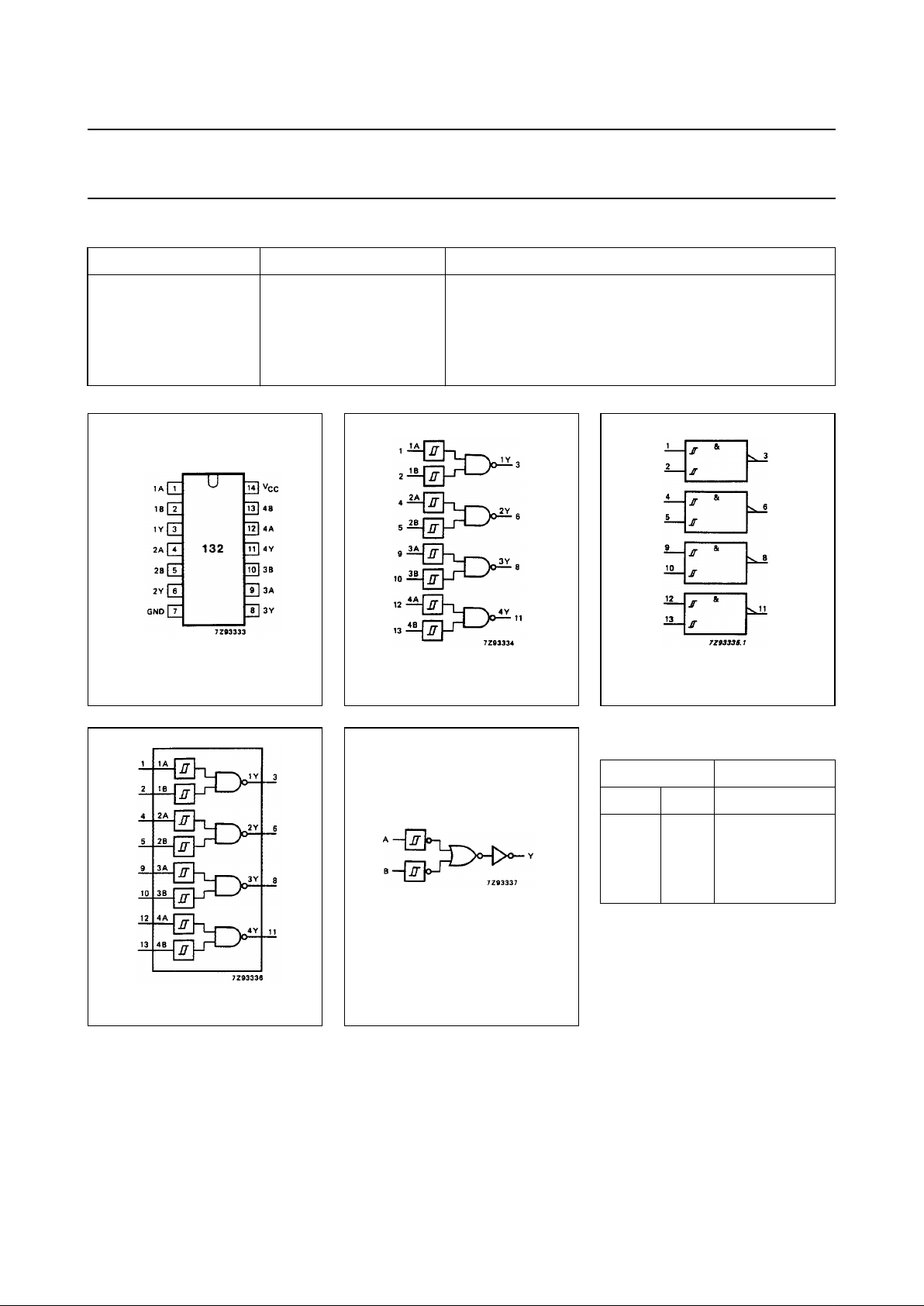
PIN DESCRIPTION
PIN NO. SYMBOL NAME AND FUNCTION
1, 4, 9, 12 1A to 4A data inputs
2, 5, 10, 13 1B to 4B data inputs
3, 6, 8, 11 1Y to 4Y data outputs
7 GND ground (0 V)
14 V
CC
positive supply voltage
Fig.1 Pin configuration. Fig.2 Logic symbol. Fig.3 IEC logic symbol.
Fig.4 Functional diagram.
Fig.5 Logic diagram
(one Schmitt trigger).
FUNCTION TABLE
Notes
1. H = HIGH voltage level
L = LOW voltage level
APPLICATIONS
• Wave and pulse shapers
• Astable multivibrators
• Monostable multivibrators
INPUTS OUTPUT
nA nB nY
LL H
LH H
HL H
HH L
 Loading...