

Philips 74HCT112DB, 74HCT112D, 74HCT112U, 74HCT112PW, 74HCT112N Datasheet
...
DATA SH EET
Product specification
Supersedes data of December 1990
File under Integrated Circuits, IC06
1998 Jun 10
INTEGRATED CIRCUITS
74HC/HCT112
Dual JK flip-flop with set and reset;
negative-edge trigger
For a complete data sheet, please also download:
•The IC06 74HC/HCT/HCU/HCMOS Logic Family Specifications
•The IC06 74HC/HCT/HCU/HCMOS Logic Package Information
•The IC06 74HC/HCT/HCU/HCMOS Logic Package Outlines

1998 Jun 10 2
Philips Semiconductors Product specification
Dual JK flip-flop with set and reset;
negative-edge trigger
74HC/HCT112
FEATURES
• Asynchronous set and reset
• Output capability: standard
• ICC category: flip-flops
GENERAL DESCRIPTION
The 74HC/HCT112 are high-speed Si-gate CMOS devices
and are pin compatible with low power Schottky TTL
(LSTTL). They are specified in compliance with JEDEC
standard no. 7A.
The 74HC/HCT112 are dual negative-edge triggered
JK-type flip-flops featuring individual nJ, nK, clock (n
CP),
set (nSD) and reset (nRD) inputs.
The set and reset inputs, when LOW, set or reset the
outputs as shown in the function table regardless of the
levels at the other inputs.
A HIGH level at the clock (n
CP) input enables the nJ and
nK inputs and data will be accepted. The nJ and nK inputs
control the state changes of the flip-flops as shown in the
function table. The nJ and nK inputs must be stable one
set-up time prior to the HIGH-to-LOW clock transition for
predictable operation.
Output state changes are initiated by the HIGH-to-LOW
transition of nCP.
Schmitt-trigger action in the clock input makes the circuit
highly tolerant to slower clock rise and fall times.
QUICK REFERENCE DATA
GND = 0 V; T
amb
=25°C; tr=tf= 6 ns
Notes
1. C
PD
is used to determine the dynamic power dissipation (PD in µW):
PD=CPD× V
CC
2
× fi+∑(CL× V
CC
2
× fo) where:
fi= input frequency in MHz
fo= output frequency in MHz
∑ (CL× V
CC
2
× fo) = sum of outputs
CL= output load capacitance in pF
VCC= supply voltage in V
2. For HC the condition is VI= GND to V
CC
For HCT the condition is VI= GND to VCC− 1.5 V
SYMBOL PARAMETER CONDITIONS
TYPICAL
UNIT
HC HCT
t
PHL
/ t
PLH
propagation delay CL= 15 pF; VCC=5 V
n
CP to nQ, nQ 1719ns
n
S
D
to nQ, nQ 1515ns
n
R
D
to nQ, nQ 1819ns
f
max
maximum clock frequency 66 70 MHz
C
I
input capacitance 3.5 3.5 pF
C
PD
power dissipation capacitance per flip-flop notes 1 and 2 27 30 pF
1998 Jun 10 3
Philips Semiconductors Product specification
Dual JK flip-flop with set and reset;
negative-edge trigger
74HC/HCT112
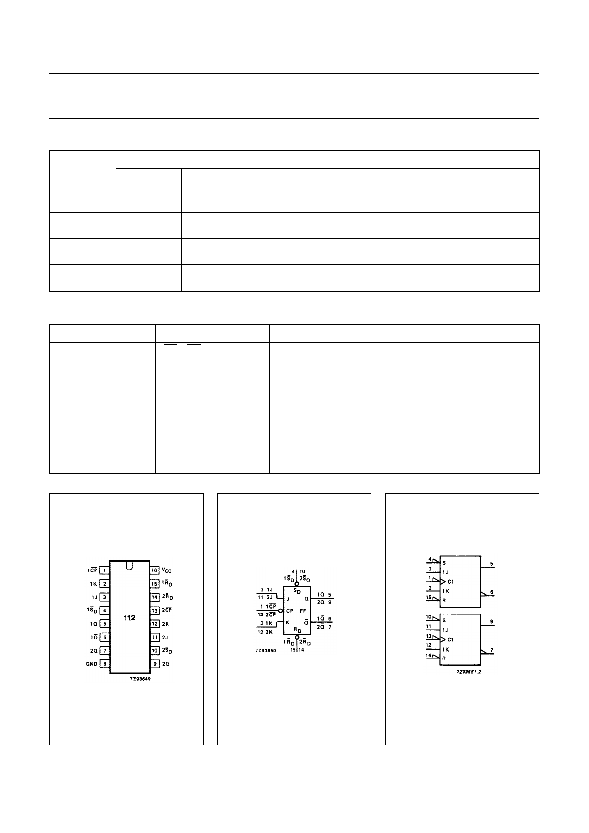
ORDERING INFORMATION
PIN DESCRIPTION
TYPE
NUMBER
PACKAGE
NAME DESCRIPTION VERSION
74HC112D;
74HCT112D
SO16 plastic small outline package; 16 leads; body width 3.9 mm SOT109-1
74HC112DB;
74HCT112DB
SSOP16 plastic shrink small outline package; 16 leads; body width 5.3 mm SOT338-1
74HC112N;
74HCT112N
DIP16 plastic dual in-line package; 16 leads (300 mil); long body SOT38-1
74HC112PW;
74HCT112PW
TSSOP16 plastic thin shrink small outline package; 16 leads; body width 4.4 mm SOT403-1
PIN NO. SYMBOL NAME AND FUNCTION
1, 13 1
CP, 2CP clock input (HIGH-to-LOW, edge triggered)
2, 12 1K, 2K data inputs; flip-flops 1 and 2
3, 11 1J, 2J data inputs; flip-flops 1 and 2
4, 10 1
SD, 2S
D
set inputs (active LOW)
5, 9 1Q, 2Q true flip-flop outputs
6, 7 1
Q, 2Q complement flip-flop outputs
8 GND ground (0 V)
15, 14 1
RD, 2R
D
reset inputs (active LOW)
16 V
CC
positive supply voltage
Fig.1 Pin configuration. Fig.2 Logic symbol. Fig.3 IEC logic symbol.
1998 Jun 10 4
Philips Semiconductors Product specification
Dual JK flip-flop with set and reset;
negative-edge trigger
74HC/HCT112
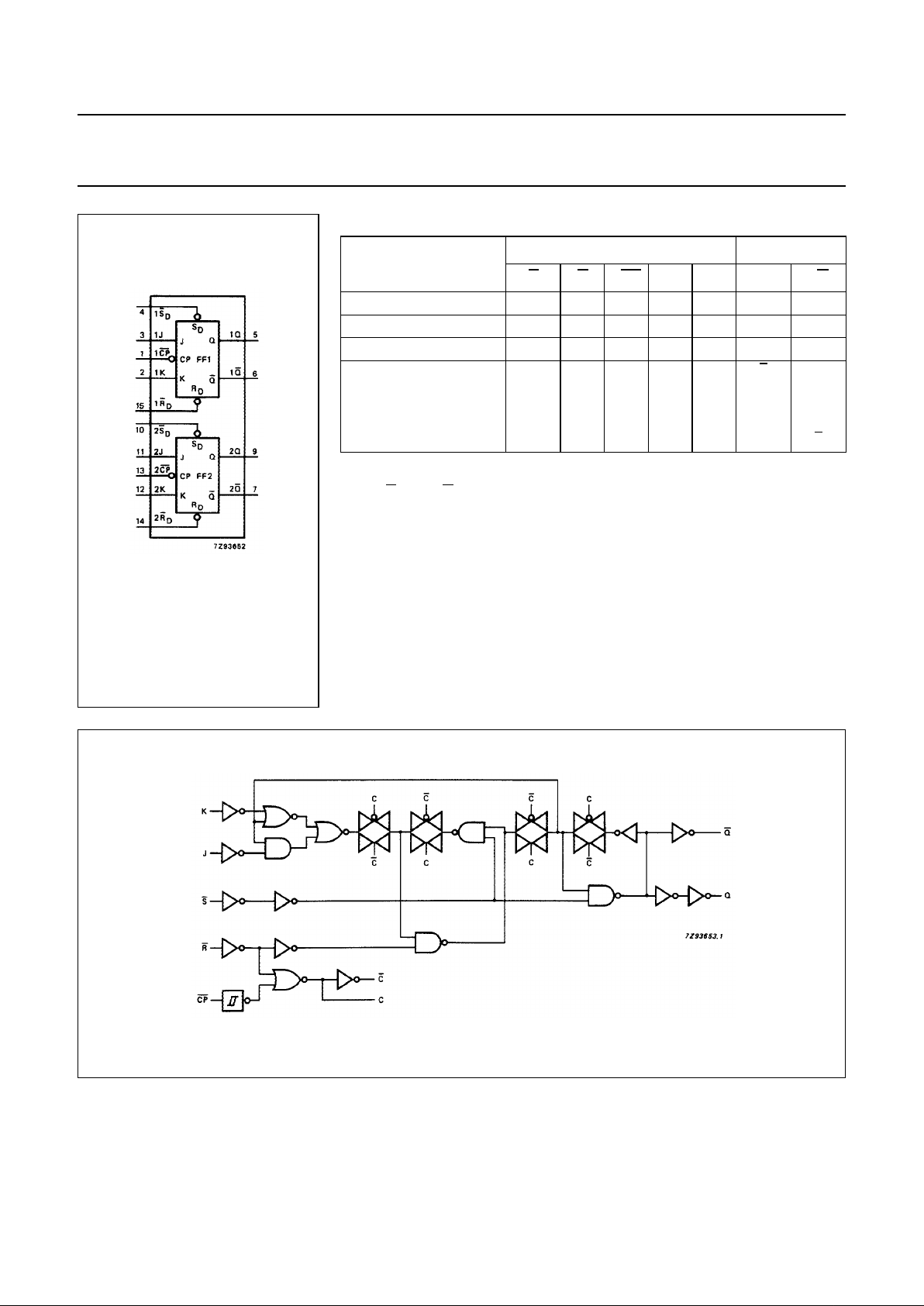
Fig.4 Functional diagram.
FUNCTION TABLE
Note
1. If n
SD and nRD simultaneously go from LOW to HIGH, the output states will
be unpredictable.
H = HIGH voltage level
h = HIGH voltage level one set-up time prior to the HIGH-to-LOW CP
transition
L = LOW voltage level
l = LOW voltage level one set-up time prior to the HIGH-to-LOW CP
transition
q = lower case letters indicate the state of the referenced output one set-up
time prior to the HIGH-to-LOW CP transition
X = don’t care
↓ = HIGH-to-LOW CP transition
OPERATING MODE
INPUTS OUTPUTS
n
SDnRDnCP nJ nK nQ nQ
asynchronous set L H X X X H L
asynchronous reset H L X X X L H
undetermined L L X X X H L
toggle H H ↓ hh
qq
load “0” (reset) H H ↓ lh L H
load “1” (set) H H ↓ hl H L
hold “no change” H H ↓ ll q
q
Fig.5 Logic diagram (one flip-flop).

1998 Jun 10 5
Philips Semiconductors Product specification
Dual JK flip-flop with set and reset;
negative-edge trigger
74HC/HCT112
DC CHARACTERISTICS FOR 74HC
For the DC characteristics see
“74HC/HCT/HCU/HCMOS Logic Family Specifications”
.
Output capability: standard
ICCcategory: flip-flops
 Loading...