

Philips 74HCT03PW, 74HCT03N, 74HCT03DB, 74HCT03D, 74HC03PW Datasheet
...
DATA SH EET
Product specification
File under Integrated Circuits, IC06
December 1990
INTEGRATED CIRCUITS
74HC/HCT03
Quad 2-input NAND gate
For a complete data sheet, please also download:
•The IC06 74HC/HCT/HCU/HCMOS Logic Family Specifications
•The IC06 74HC/HCT/HCU/HCMOS Logic Package Information
•The IC06 74HC/HCT/HCU/HCMOS Logic Package Outlines
December 1990 2
Philips Semiconductors Product specification
Quad 2-input NAND gate 74HC/HCT03
FEATURES
• Level shift capability
• Output capability: standard (open drain)
• ICC category: SSI
GENERAL DESCRIPTION
The 74HC/HCT03 are high-speed Si-gate CMOS devices
and are pin compatible with low power Schottky TTL
(LSTTL). They are specified in compliance with JEDEC
standard no. 7A.
The 74HC/HCT03 provide the 2-input NAND function.
The 74HC/HCT03 have open-drain N-transistor outputs,
which are not clamped by a diode connected to V
CC
. In
the OFF-state, i.e. when one input is LOW, the output
may be pulled to any voltage between GND and V
Omax
.
This allows the device to be used as a LOW-to-HIGH or
HIGH-to-LOW level shifter. For digital operation and
OR-tied output applications, these devices must have a
pull-up resistor to establish a logic HIGH level.
QUICK REFERENCE DATA
GND = 0 V; T
amb
=25°C; tr=tf= 6 ns
Notes
1. C
PD
is used to determine the dynamic power dissipation (PD in µW):
PD=CPD × V
CC
2
× fi+ ∑ (CL× V
CC
2
× fo) + ∑ (V
O
2
/RL) × duty factor LOW, where:
fi= input frequency in MHz
fo= output frequency in MHz
VO= output voltage in V
CL= output load capacitance in pF
VCC= supply voltage in V
RL= pull-up resistor in MΩ
∑ (CL× V
CC
2
× fo) = sum of outputs
∑ (V
O
2
/RL) = sum of outputs
2. For HC the condition is VI= GND to V
CC
For HCT the condition is VI= GND to VCC− 1.5 V
3. The given value of CPD is obtained with:
CL= 0 pF and RL= ∞
ORDERING INFORMATION
See
“74HC/HCT/HCU/HCMOS Logic Package Information”
.
SYMBOL PARAMETER CONDITIONS
TYPICAL
UNIT
HC HCT
t
PZL
/ t
PLZ
propagation delay CL= 15 pF; RL=1 kΩ; VCC= 5 V 8 10 ns
C
I
input capacitance 3.5 3.5 pF
C
PD
power dissipation capacitance per gate notes 1, 2 and 3 4.0 4.0 pF
December 1990 3
Philips Semiconductors Product specification
Quad 2-input NAND gate 74HC/HCT03
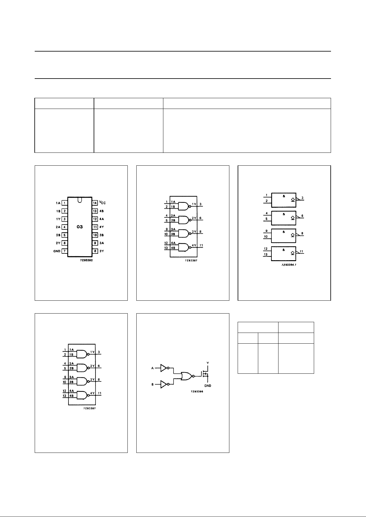
PIN DESCRIPTION
PIN NO. SYMBOL NAME AND FUNCTION
1, 4, 9, 12 1A to 4A data inputs
2, 5, 10, 13 1B to 4B data inputs
3, 6, 8, 11 1Y to 4Y data outputs
7 GND ground (0 V)
14 V
CC
positive supply voltage
Fig.1 Pin configuration. Fig.2 Logic symbol. Fig.3 IEC logic symbol.
Fig.4 Functional diagram. Fig.5 Logic diagram (one gate).
FUNCTION TABLE
Note
1. H = HIGH voltage level
L = LOW voltage level
Z = high impedance OFF-state
INPUTS OUTPUT
nA nB nY
L
L
H
H
L
H
L
H
Z
Z
Z
L
 Loading...