

查询74HC00供应商
INTEGRATED CIRCUITS
DATA SH EET
74HC00; 74HCT00
Quad 2-input NAND gate
Product specification
Supersedes data of 1997 Aug 26
2003 Jun 30
Philips Semiconductors Product specification
Quad 2-input NAND gate 74HC00; 74HCT00
FEATURES
• Complies with JEDEC standard no. 8-1A
• ESD protection:
HBM EIA/JESD22-A114-A exceeds 2000 V
MM EIA/JESD22-A115-A exceeds 200 V
• Specified from −40 to +85 °C and −40 to +125 °C.
DESCRIPTION
The 74HC00/74HCT00 are high-speed Si-gate CMOS
devices and are pin compatible with low power Schottky
TTL (LSTTL). They are specified in compliance with
JEDEC standard no. 7A.
The 74HC00/74HCT00 provide the 2-input NAND
function.
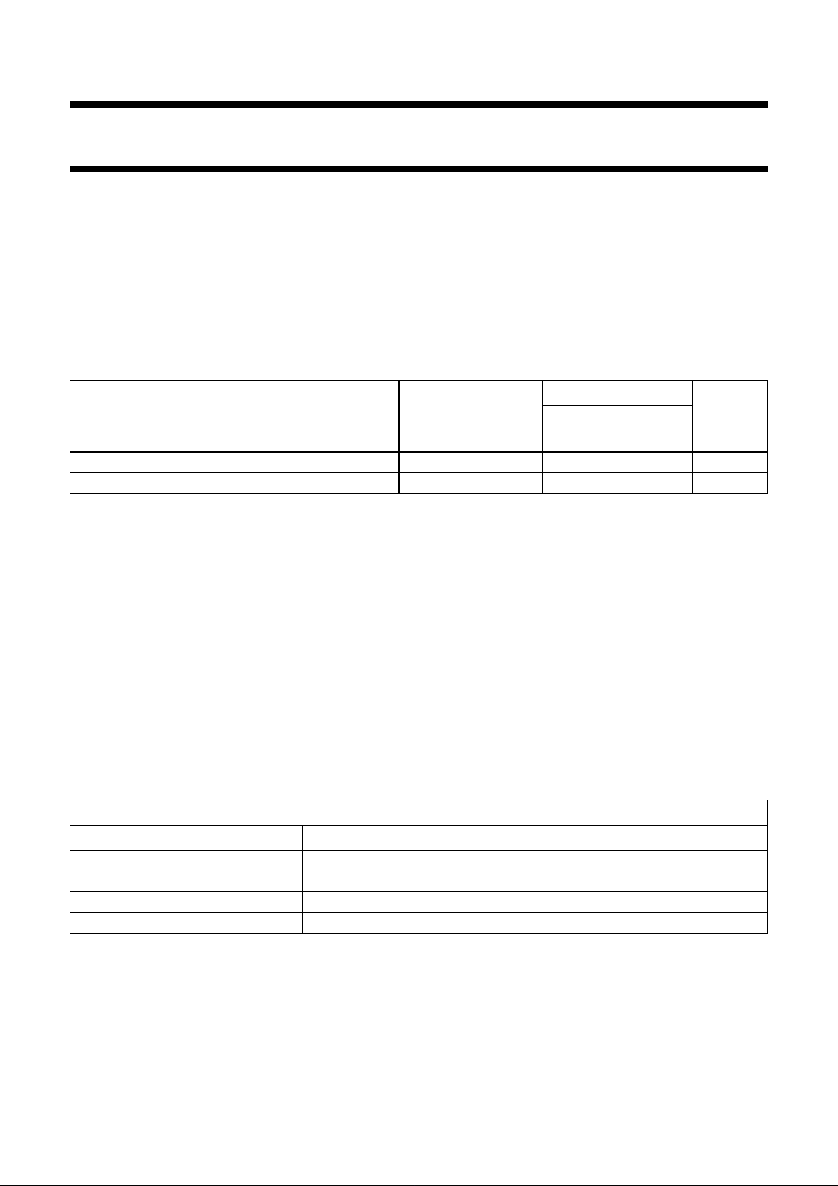
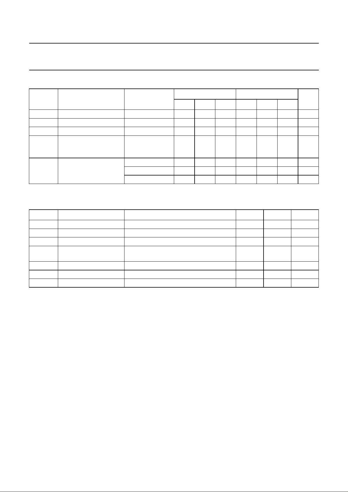
QUICK REFERENCE DATA
GND = 0 V; T
=25°C; tr=tf= 6 ns.
amb
SYMBOL PARAMETER CONDITIONS
t
PHL/tPLH
C
I
C
PD
propagation delay nA, nB to nY CL= 15 pF; VCC= 5 V 7 10 ns
input capacitance 3.5 3.5 pF
power dissipation capacitance per gate notes 1 and 2 22 22 pF
Notes
1. C
is used to determine the dynamic power dissipation (PDin µW).
PD
PD=CPD× V
2
× fi× N+Σ(CL× V
CC
2
× fo) where:
CC
fi= input frequency in MHz;
fo= output frequency in MHz;
= output load capacitance in pF;
C
L
VCC= supply voltage in Volts;
N = total load switching outputs;
Σ(CL× V
2
× fo) = sum of the outputs.
CC
2. For 74HC00 the condition is VI= GND to VCC.
For 74HCT00 the condition is VI= GND to VCC− 1.5 V.
TYPICAL
UNIT
74HC00 74HCT00
FUNCTION TABLE
See note 1.
INPUT OUTPUT
nA nB nY
LLH
LHH
HLH
HHL
Note
1. H = HIGH voltage level;
L = LOW voltage level.
2003 Jun 30 2
Philips Semiconductors Product specification
Quad 2-input NAND gate 74HC00; 74HCT00
ORDERING INFORMATION
PACKAGE
TYPE NUMBER
74HC00N −40to+125°C 14 DIP14 plastic SOT27-1
74HCT00N −40 to +125 °C 14 DIP14 plastic SOT27-1
74HC00D −40to+125°C 14 SO14 plastic SOT108-1
74HCT00D −40 to +125 °C 14 SO14 plastic SOT108-1
74HC00DB −40 to +125 °C 14 SSOP14 plastic SOT337-1
74HCT00DB −40 to +125 °C 14 SSOP14 plastic SOT337-1
74HC00PW −40 to +125 °C 14 TSSOP14 plastic SOT402-1
74HCT00PW −40 to +125 °C 14 TSSOP14 plastic SOT402-1
74HC00BQ −40 to +125 °C 14 DHVQFN14 plastic SOT762-1
74HCT00BQ −40 to +125 °C 14 DHVQFN14 plastic SOT762-1
TEMPERATURE
RANGE
PINS PACKAGE MATERIAL CODE
PINNING
PIN SYMBOL DESCRIPTION
1 1A data input
2 1B data input
3 1Y data output
4 2A data input
5 2B data input
6 2Y data output
7 GND ground (0 V)
8 3Y data output
9 3A data input
10 3B data input
11 4Y data output
12 4A data input
13 4B data input
14 V
CC
supply voltage
handbook, halfpage
1A
1B
1Y
2A
2B
2Y
GND
1
2
3
4
00
5
6
7
14
13
12
11
10
9
8
MNA210
Fig.1 Pin configuration DIP14, SO14 and
(T)SSOP14.
V
4B
4A
4Y
3B
3A
3Y
CC
2003 Jun 30 3
Philips Semiconductors Product specification
Quad 2-input NAND gate 74HC00; 74HCT00
V
handbook, halfpage
1B
2
1A
CC
114
13
4B
3
1Y
4
2A
5
2B
6
2Y
Top view
(1) The die substrate is attached to this pad using conductive die
attach material. It can not be used as a supply pin or input.
(1)
GND
7
GND 3Y
8
12
11
10
9
MNA950
4A
4Y
3B
3A
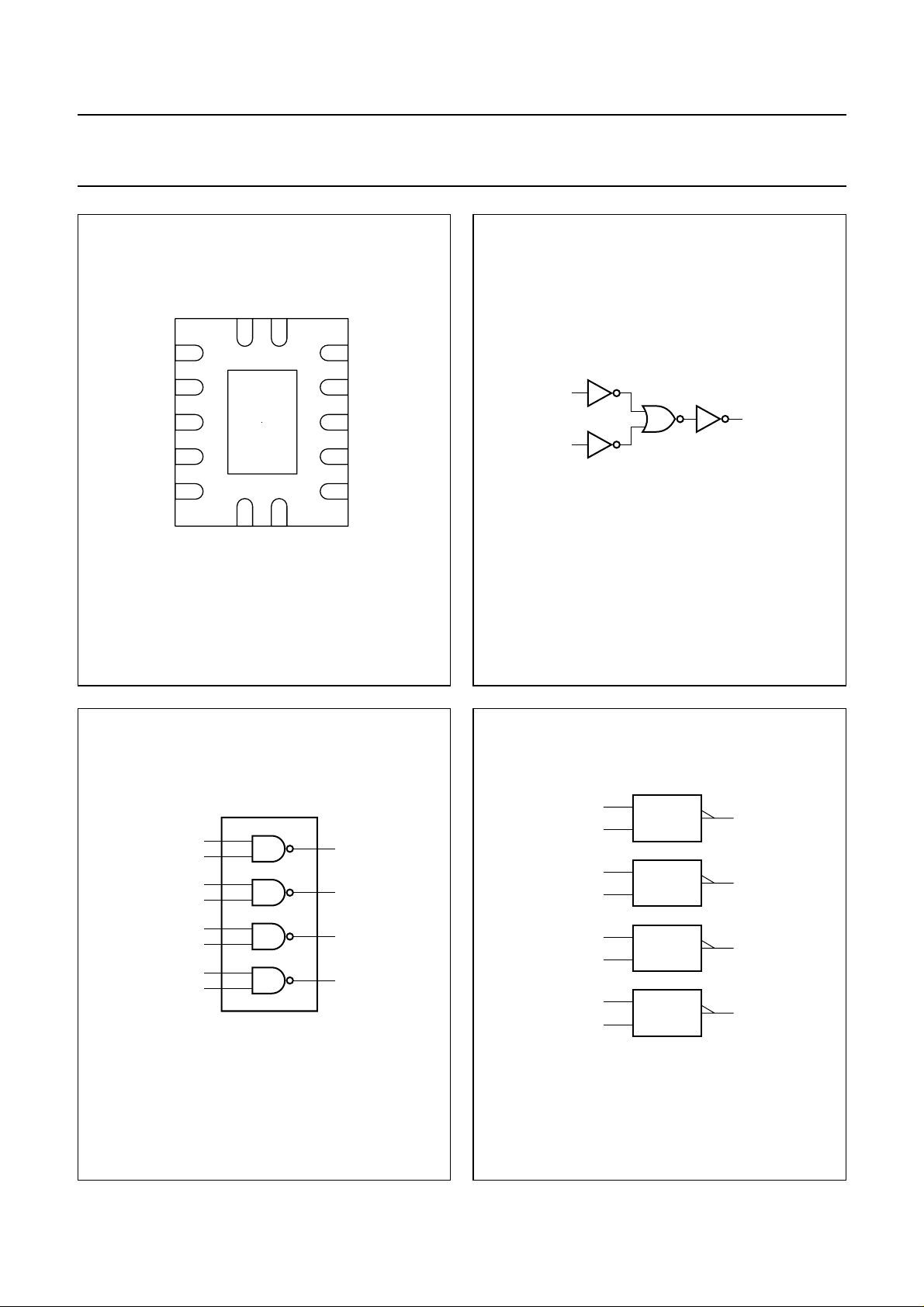
Fig.2 Pin configuration DHVQFN14.
handbook, halfpage
1
1B
2
4
2B
5
1Y1A3
2Y2A6
handbook, halfpage
handbook, halfpage
A
Y
B
MNA211
Fig.3 Logic diagram (one gate).
1
2
4
5
&
&
3
6
9
3B
10
12
4B
13
3Y3A8
4Y4A11
MNA212
Fig.4 Function diagram.
2003 Jun 30 4
9
10
12
13
&
&
MNA246
8
11
Fig.5 IEC logic symbol.
Philips Semiconductors Product specification
Quad 2-input NAND gate 74HC00; 74HCT00
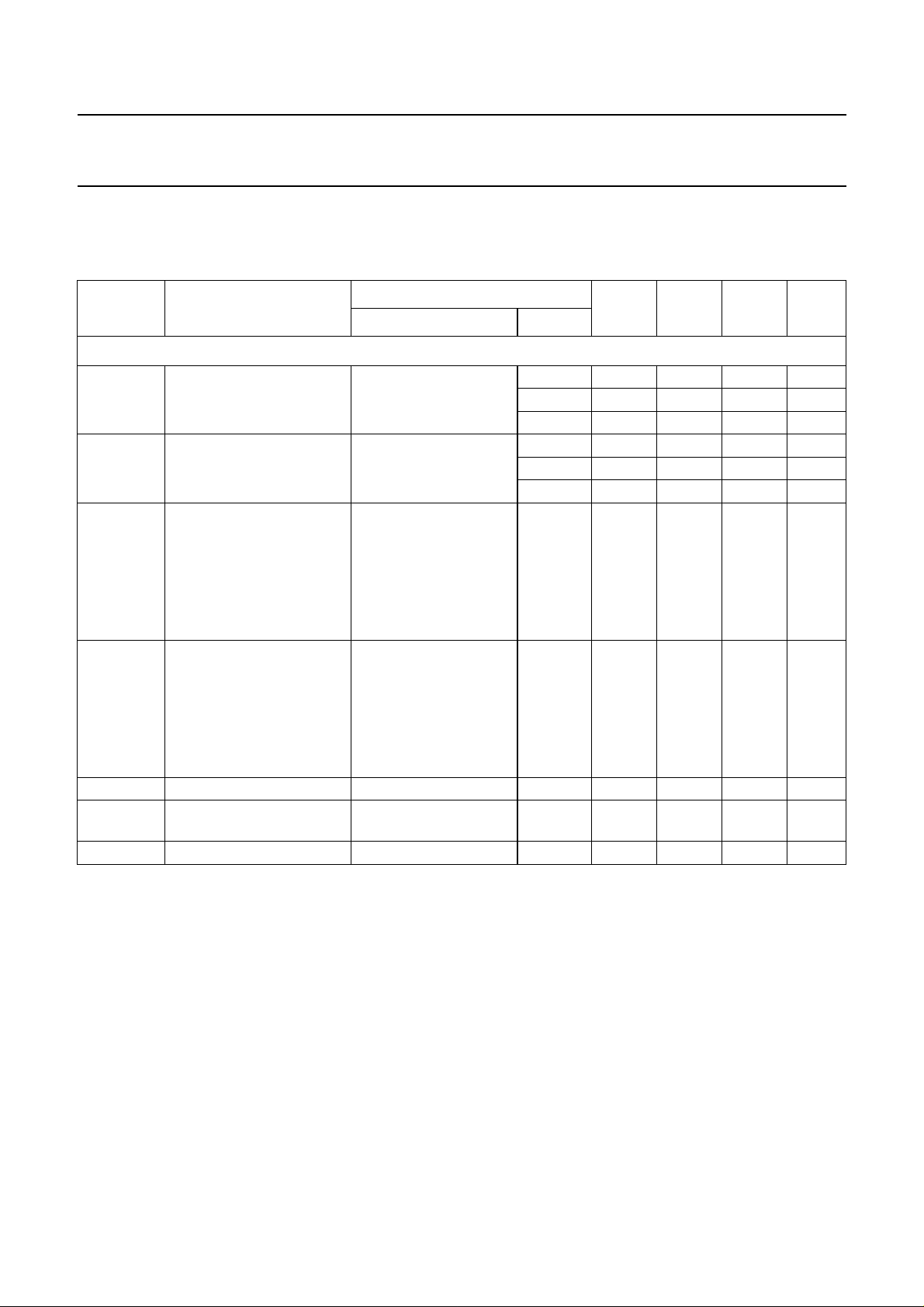
RECOMMENDED OPERATING CONDITIONS
SYMBOL PARAMETER CONDITIONS
UNIT
MIN. TYP. MAX. MIN. TYP. MAX.
74HC00 74HCT00
V
CC
V
I
V
O
T
amb
supply voltage 2.0 5.0 6.0 4.5 5.0 5.5 V
input voltage 0 − V
output voltage 0 − V
operating ambient
temperature
see DC and AC
characteristicsper
−40 +25 +125 −40 +25 +125 °C
0 − V
CC
0 − V
CC
CC
CC
V
V
device
t
r,tf
input rise and fall times VCC= 2.0 V −−1000 −−−ns
= 4.5 V − 6.0 500 − 6.0 500 ns
V
CC
V
= 6.0 V −−400 −−−ns
CC
LIMITING VALUES
In accordance with theAbsolute Maximum Rating System (IEC 60134); voltages are referenced to GND (ground = 0 V).
SYMBOL PARAMETER CONDITIONS MIN. MAX. UNIT
V
CC
I
IK
I
OK
I
O
supply voltage −0.5 +7.0 V
input diode current VI< −0.5 V or VI>VCC+ 0.5 V −±20 mA
output diode current VO< −0.5 V or VO>VCC+ 0.5 V −±20 mA
output source or sink
−0.5V<VO<VCC+ 0.5 V −±25 mA
current
I
, I
CC
T
stg
P
tot
GNDVCC
or GND current −±50 mA
storage temperature −65 +150 °C
power dissipation T
= −40 to +125 °C; note 1 − 500 mW
amb
Note
1. For DIP14 packages: above 70 °C derate linearly with 12 mW/K.
For SO14 packages: above 70 °C derate linearly with 8 mW/K.
For SSOP14 and TSSOP14 packages: above 60 °C derate linearly with 5.5 mW/K.
For DHVQFN14 packages: above 60 °C derate linearly with 4.5 mW/K.
2003 Jun 30 5
Philips Semiconductors Product specification
Quad 2-input NAND gate 74HC00; 74HCT00
DC CHARACTERISTICS
Type 74HC00
At recommended operating conditions; voltages are referenced to GND (ground=0V).
SYMBOL PARAMETER
T
= −40 to +85 °C; note 1
amb
V
IH
V
IL
V
OH
V
OL
I
LI
I
OZ
I
CC
HIGH-level input voltage 2.0 1.5 1.2 − V
LOW-level input voltage 2.0 − 0.8 0.5 V
HIGH-level output voltage VI=VIH or V
LOW-level output voltage VI=VIH or V
input leakage current VI=VCC or GND 6.0 −−±1.0 µA
3-state output OFF current VI=VIH or VIL;
quiescent supply current VI=VCC or GND; IO= 0 6.0 −−20 µA
TEST CONDITIONS
MIN. TYP. MAX. UNIT
OTHER V
CC
(V)
4.5 3.15 2.4 − V
6.0 4.2 3.2 − V
4.5 − 2.1 1.35 V
6.0 − 2.8 1.8 V
IL
IO= −20 µA 2.0 1.9 2.0 − V
I
= −20 µA 4.5 4.4 4.5 − V
O
I
= −20 µA 6.0 5.9 6.0 − V
O
I
= −4.0 mA 4.5 3.84 4.32 − V
O
I
= −5.2 mA 6.0 5.34 5.81 − V
O
IL
IO=20µA 2.0 − 0 0.1 V
I
=20µA 4.5 − 0 0.1 V
O
I
=20µA 6.0 − 0 0.1 V
O
I
= 4.0 mA 4.5 − 0.15 0.33 V
O
I
= 5.2 mA 6.0 − 0.16 0.33 V
O
6.0 −−±.5.0 µA
VO=VCC or GND
2003 Jun 30 6

Philips Semiconductors Product specification
Quad 2-input NAND gate 74HC00; 74HCT00
SYMBOL PARAMETER
T
= −40 to +125 °C
amb
V
IH
V
IL
V
OH
V
OL
I
LI
I
OZ
I
CC
HIGH-level input voltage 2.0 1.5 −−V
LOW-level input voltage 2.0 −−0.5 V
HIGH-level output voltage VI=VIH or V
LOW-level output voltage VI=VIH or V
input leakage current VI=VCC or GND 6.0 −−±1.0 µA
3-state output OFF current VI=VIH or VIL;
quiescent supply current VI=VCC or GND; IO= 0 6.0 −−40 µA
Note
1. All typical values are measured at T
TEST CONDITIONS
MIN. TYP. MAX. UNIT
OTHER V
CC
(V)
4.5 3.15 −−V
6.0 4.2 −−V
4.5 −−1.35 V
6.0 −−1.8 V
IL
IO= −20 µA 2.0 1.9 −−V
I
=−20 µA 4.5 4.4 −−V
O
I
=−20 µA 6.0 5.9 −−V
O
=−4.0 mA 4.5 3.7 −−V
I
O
I
=−5.2 mA 6.0 5.2 −−V
O
IL
IO=20µA 2.0 −−0.1 V
I
=20µA 4.5 −−0.1 V
O
=20µA 6.0 −−0.1 V
I
O
I
= 4.0 mA 4.5 −−0.4 V
O
I
= 5.2 mA 6.0 −−0.4 V
O
6.0 −−±10.0 µA
VO=VCC or GND
=25°C.
amb
2003 Jun 30 7

Philips Semiconductors Product specification
Quad 2-input NAND gate 74HC00; 74HCT00
Type 74HCT00
At recommended operating conditions; voltages are referenced to GND (ground=0V).
SYMBOL PARAMETER
T
= −40 to +85 °C; note 1
amb
V
IH
V
IL
V
OH
V
OL
I
LI
I
OZ
I
CC
∆I
CC
T
= −40 to +125 °C
amb
V
IH
V
IL
V
OH
V
OL
I
LI
I
OZ
I
CC
∆I
CC
HIGH-level input voltage 4.5 to 5.5 2.0 1.6 − V
LOW-level input voltage 4.5 to 5.5 − 1.2 0.8 V
HIGH-level output voltage VI=VIH or V
LOW-level output voltage VI=VIH or V
input leakage current VI=VCC or GND 5.5 −−±1.0 µA
3-state output OFF current VI=VIHor VIL;
quiescent supply current VI=VCC or GND;
additional supply current per input VI=VCC− 2.1 V;
HIGH-level input voltage 4.5 to 5.5 2.0 −−V
LOW-level input voltage 4.5 to 5.5 −−0.8 V
HIGH-level output voltage VI=VIH or V
LOW-level output voltage VI=VIH or V
input leakage current VI=VCCor GND 5.5 −−±1.0 µA
3-state output OFF current VI=VIH or VIL;
quiescent supply current VI=VCC or GND;
additional supply current per input VI=VCC− 2.1 V;
TEST CONDITIONS
MIN. TYP. MAX. UNIT
OTHER V
IL
CC
(V)
IO= −20 µA 4.5 4.4 4.5 − V
I
= −4.0 mA 4.5 3.84 4.32 − V
O
IL
IO=20µA 4.5 − 0 0.1 V
= 4.0 mA 4.5 − 0.15 0.33 V
I
O
5.5 −−±5.0 µA
VO=VCCor GND;
IO=0
5.5 −−20 µA
IO=0
4.5 to 5.5 − 150 675 µA
IO=0
IL
IO= −20 µA 4.5 4.4 −−V
I
=−4.0 mA 4.5 3.7 −−V
O
IL
IO=20µA 4.5 −−0.1 V
I
= 4.0 mA 4.5 −−0.4 V
O
5.5 −−±10 µA
VO=VCCor GND;
IO=0
5.5 −−40 µA
IO=0
4.5 to 5.5 −−735 µA
IO=0
Note
1. All typical values are measured at T
amb
=25°C.
2003 Jun 30 8

Philips Semiconductors Product specification
Quad 2-input NAND gate 74HC00; 74HCT00
AC CHARACTERISTICS
Type 74HC00
GND = 0 V; tr=tf= 6 ns; CL=50pF.
SYMBOL PARAMETER
T
= −40 to +85 °C; note 1
amb
t
PHL/tPLH
t
THL/tTLH
T
amb
t
PHL/tPLH
t
THL/tTLH
propagation delay nA, nB to nY see Fig.6 2.0 − 25 115 ns
output transition time 2.0 − 19 95 ns
= −40 to +125 °C
propagation delay nA, nB to nY see Fig.6 2.0 −−135 ns
output transition time 2.0 −−110 ns
Note
1. All typical values are measured at T
amb
TEST CONDITIONS
MIN. TYP. MAX. UNIT
WAVEFORMS V
CC
(V)
see Fig.6 4.5 − 923ns
see Fig.6 6.0 − 720ns
4.5 − 719ns
6.0 − 616ns
see Fig.6 4.5 −−27 ns
see Fig.6 6.0 −−23 ns
4.5 −−22 ns
6.0 −−19 ns
=25°C.
Type 74HCT00
GND = 0 V; tr=tf= 6 ns; CL=50pF
SYMBOL PARAMETER
T
= −40 to +85 °C; note 1
amb
t
PHL/tPLH
t
THL/tTLH
T
amb
t
PHL/tPLH
t
THL/tTLH
propagation delay nA, nB to nY see Fig.6 4.5 − 12 24 ns
output transition time 4.5 −−29 ns
= −40 to +125 °C
propagation delay nA, nB to nY see Fig.6 4.5 −−29 ns
output transition time 4.5 −−22 ns
Note
1. All typical values are measured at T
amb
=25°C.
TEST CONDITIONS
WAVEFORMS V
CC
MIN. TYP MAX. UNIT
(V)
2003 Jun 30 9

Philips Semiconductors Product specification
Quad 2-input NAND gate 74HC00; 74HCT00
AC WAVEFORMS
handbook, halfpage
74HC00: VM= 50%; VI= GND to VCC.
74HCT00: VM= 1.3 V; VI= GND to 3 V.
Fig.6 Waveforms showing the input (nA, nB) to output (nY) propagation delays.
nA, nB input
nY output
GND
V
OH
V
OL
V
I
V
M
t
PHL
V
M
t
THL
t
PLH
t
TLH
MNA218
2003 Jun 30 10

Philips Semiconductors Product specification
Quad 2-input NAND gate 74HC00; 74HCT00
PACKAGE OUTLINES
DIP14: plastic dual in-line package; 14 leads (300 mil)
SOT27-1
seating plane
L
Z
14
pin 1 index
1
D
A
2
A
A
1
e
b
w M
b
1
8
E
7
M
E
c
(e )
1
M
H
0 5 10 mm
scale
DIMENSIONS (inch dimensions are derived from the original mm dimensions)
A
UNIT
mm
inches
Note
1. Plastic or metal protrusions of 0.25 mm (0.01 inch) maximum per side are not included.
max.
OUTLINE
VERSION
SOT27-1
A
min.
A
1 2
max.
IEC JEDEC JEITA
050G04 MO-001 SC-501-14
b
1.73
1.13
0.068
0.044
b
0.53
0.38
0.021
0.015
1
cD
0.36
0.23
0.014
0.009
REFERENCES
(1) (1)
19.50
18.55
0.77
0.73
Ee M
6.48
6.20
0.26
0.24
2003 Jun 30 11
M
e
L
1
3.60
3.05
0.14
0.12
E
8.25
7.80
0.32
0.31
EUROPEAN
PROJECTION
10.0
8.3
0.39
0.33
H
0.2542.54 7.62
ISSUE DATE
w
0.010.1 0.3
99-12-27
03-02-13
max.
2.24.2 0.51 3.2
0.0870.17 0.02 0.13
(1)
Z

Philips Semiconductors Product specification
Quad 2-input NAND gate 74HC00; 74HCT00
SO14: plastic small outline package; 14 leads; body width 3.9 mm
D
c
y
Z
14
pin 1 index
1
e
8
A
2
7
w M
b
p
SOT108-1
E
H
E
A
1
L
detail X
A
X
v M
A
Q
(A )
A
3
θ
L
p
0 2.5 5 mm
scale
DIMENSIONS (inch dimensions are derived from the original mm dimensions)
UNIT
mm
inches
A
max.
1.75
0.069
A
1
0.25
0.10
0.010
0.004
A2A
1.45
1.25
0.057
0.049
0.25
0.01
b
3
p
0.49
0.25
0.36
0.19
0.019
0.0100
0.014
0.0075
(1)E(1)
cD
8.75
8.55
0.35
0.34
eHELLpQZywv θ
4.0
1.27
3.8
0.16
0.15
0.05
0.244
0.228
Note
1. Plastic or metal protrusions of 0.15 mm (0.006 inch) maximum per side are not included.
OUTLINE
VERSION
SOT108-1
IEC JEDEC JEITA
076E06 MS-012
REFERENCES
2003 Jun 30 12
6.2
5.8
1.05
0.041
1.0
0.4
0.039
0.016
0.7
0.25
0.6
0.028
0.01 0.004
0.024
EUROPEAN
PROJECTION
0.25 0.1
0.01
(1)
0.7
0.3
0.028
0.012
ISSUE DATE
99-12-27
03-02-19
o
8
o
0

Philips Semiconductors Product specification
Quad 2-input NAND gate 74HC00; 74HCT00
SSOP14: plastic shrink small outline package; 14 leads; body width 5.3 mm
D
c
y
Z
14
pin 1 index
8
A
2
A
E
H
E
1
SOT337-1
A
X
v M
A
Q
(A )
L
p
L
A
3
θ
p
7
b
p
cD
0.20
0.09
REFERENCES
MO-150
w M
0 2.5 5 mm
scale
(1)E(1)
6.4
5.4
6.0
0.65 1.25 0.2
5.2
1
e
DIMENSIONS (mm are the original dimensions)
mm
OUTLINE
VERSION
SOT337-1
A
max.
2
0.21
0.05
1.80
1.65
IEC JEDEC JEITA
0.25
0.38
0.25
UNIT A1A2A3b
Note
1. Plastic or metal protrusions of 0.25 mm maximum per side are not included.
2003 Jun 30 13
detail X
eHELLpQZywv θ
7.9
7.6
1.03
0.63
0.9
0.7
EUROPEAN
PROJECTION
0.13 0.1
(1)
1.4
0.9
ISSUE DATE
99-12-27
03-02-19
o
8
o
0

Philips Semiconductors Product specification
Quad 2-input NAND gate 74HC00; 74HCT00
TSSOP14: plastic thin shrink small outline package; 14 leads; body width 4.4 mm
D
c
y
Z
14
pin 1 index
8
17
w
b
e
p
M
A
2
A
1
E
H
E
L
detail X
SOT402-1
A
X
v
M
A
Q
(A )
3
A
θ
L
p
0 2.5 5 mm
scale
DIMENSIONS (mm are the original dimensions)
UNIT A1A2A
Notes
1. Plastic or metal protrusions of 0.15 mm maximum per side are not included.
2. Plastic interlead protrusions of 0.25 mm maximum per side are not included.
A
max.
0.15
mm
1.1
OUTLINE
VERSION
SOT402-1 MO-153
0.05
0.95
0.80
IEC JEDEC JEITA
0.25
b
3
p
0.30
0.19
(1)E(2) (1)
cD
0.2
5.1
4.5
0.1
REFERENCES
4.9
4.3
0.65
2003 Jun 30 14
eHELLpQZywv θ
6.6
6.2
0.75
0.50
0.4
0.3
EUROPEAN
PROJECTION
0.13 0.10.21
0.72
0.38
ISSUE DATE
99-12-27
03-02-18
o
8
o
0

Philips Semiconductors Product specification
Quad 2-input NAND gate 74HC00; 74HCT00
DHVQFN14: plastic dual in-line compatible thermal enhanced very thin quad flat package; no leads;
14 terminals; body 2.5 x 3 x 0.85 mm
A
D
B
A
A
E
1
SOT762-1
c
terminal 1
index area
terminal 1
index area
L
1
E
h
14
DIMENSIONS (mm are the original dimensions)
(1)
A
UNIT
mm
Note
1. Plastic or metal protrusions of 0.075 mm maximum per side are not included.
max.
A
0.05
0.00
b
1
0.30
0.18
e
26
13
c
0.2
e
1
b
9
D
h
0 2.5 5 mm
D
3.1
2.9
(1)
1.65
1.35
(1)
E
2.6
2.4
E
1.15
0.85
h
D
h
v
w
7
e
8
scale
0.51
detail X
C
M
ACCB
M
e
L
1
0.5
2
0.3
y
w
0.1v0.05
C
1
ye
y
0.05 0.1
1
y
X
OUTLINE
VERSION
SOT762-1 MO-241 - - -- - -
IEC JEDEC JEITA
REFERENCES
2003 Jun 30 15
EUROPEAN
PROJECTION
ISSUE DATE
02-10-17
03-01-27

Philips Semiconductors Product specification
Quad 2-input NAND gate 74HC00; 74HCT00
DATA SHEET STATUS
LEVEL
DATA SHEET
STATUS
(1)
PRODUCT
STATUS
(2)(3)
DEFINITION
I Objective data Development This data sheet contains data from the objective specification for product
development. Philips Semiconductors reserves the right to change the
specification in any manner without notice.
II Preliminary data Qualification This data sheet contains data from the preliminary specification.
Supplementary data will be published at a later date. Philips
Semiconductors reserves the right to change the specification without
notice, in order to improve the design and supply the best possible
product.
III Product data Production This data sheet contains data from the product specification. Philips
Semiconductors reserves the right to make changes at any time in order
to improve the design, manufacturing and supply. Relevant changes will
be communicated via a Customer Product/Process Change Notification
(CPCN).
Notes
1. Please consult the most recently issued data sheet before initiating or completing a design.
2. The product status of the device(s) described in this data sheet may have changed since this data sheet was
published. The latest information is available on the Internet at URL http://www.semiconductors.philips.com.
3. For data sheets describing multiple type numbers, the highest-level product status determines the data sheet status.
DEFINITIONS
DISCLAIMERS
Short-form specification The data in a short-form
specification is extracted from a full data sheet with the
same type number and title. For detailed information see
the relevant data sheet or data handbook.
Limiting values definition Limiting values given are in
accordance with the Absolute Maximum Rating System
(IEC 60134). Stress above one or more of the limiting
values may cause permanent damage to the device.
These are stress ratings only and operation of the device
attheseorat any other conditions above those given in the
Characteristics sections of the specification is not implied.
Exposure to limiting values for extended periods may
affect device reliability.
Application information Applications that are
described herein for any of these products are for
illustrative purposes only. Philips Semiconductors make
norepresentationorwarrantythatsuchapplicationswillbe
suitable for the specified use without further testing or
modification.
Life support applications These products are not
designed for use in life support appliances, devices, or
systems where malfunction of these products can
reasonably be expected to result in personal injury.Philips
Semiconductorscustomersusingorsellingtheseproducts
for use in such applications do so at their own risk and
agree to fully indemnify Philips Semiconductors for any
damages resulting from such application.
Right to make changes Philips Semiconductors
reserves the right to make changes in the products including circuits, standard cells, and/or software described or contained herein in order to improve design
and/or performance. When the product is in full production
(status ‘Production’), relevant changes will be
communicated via a Customer Product/Process Change
Notification (CPCN). Philips Semiconductors assumes no
responsibility or liability for the use of any of these
products, conveys no licence or title under any patent,
copyright, or mask work right to these products, and
makes no representations or warranties that these
products are free from patent, copyright, or mask work
right infringement, unless otherwise specified.
2003 Jun 30 16

Philips Semiconductors – a w orldwide compan y
Contact information
For additional information please visit http://www.semiconductors.philips.com. Fax: +31 40 27 24825
For sales offices addresses send e-mail to: sales.addresses@www.semiconductors.philips.com.
© Koninklijke Philips Electronics N.V. 2003
All rights are reserved. Reproduction in whole or in part is prohibited without the prior written consent of the copyright owner.
The information presented in this document does not form part of any quotation or contract, is believed to be accurate and reliable and may be changed
without notice. No liability will be accepted by the publisher for any consequence of its use. Publication thereof does not convey nor imply any license
under patent- or other industrial or intellectual property rights.
Printed in The Netherlands 613508/03/pp17 Date of release: 2003 Jun 30 Document order number: 9397 750 11258
SCA75
 Loading...