

Philips 74f841, 74f842, 74f 843, 74f 845, 74f846 DATASHEETS
INTEGRATED CIRCUITS
74F841/842/843/845/846
Bus interface latches
Product specification
Replaces datasheet 74F841/842/843/844/845/846 of 1999 Jan 08
IC15 Data Handbook
1999 Jun 23
Philips Semiconductors Product specification
Bus interface latches
74F841/74F842/74F843/
74F841/74F842 10-bit bus interface latches, non-inverting/inverting (3-State)
74F843 9-bit bus interface latch, non-inverting (3-State)
74F845/74F846 8-bit bus interface latches, non-inverting/inverting (3-State)
FEA TURES
•High speed parallel latches
•Extra data width for wide address/data paths or buses carrying
parity
•High impedance NPN base input structure minimizes bus loading
•IIL is 20µA vs 1000A for AM29841 series
•Buffered control inputs to reduce AC effects
•Ideal where high speed, light loading, or increased fan-in are
required as with MOS microprocessors
•Positive and negative over-shoots are clamped to ground
•3-State outputs glitch free during power-up and power-down
•48mA sink current
•Slim dual in-line 300 mil package
•Broadside pinout
•Pin-for-pin and function compatible with AMD AM29841-846
series
TYPICAL
TYPE
74F841, 74F842 5.5ns 60mA
74F843, 74F845 5.5ns 75mA
74F846 6.2ns 60mA
PROPAGATION
DELA Y
TYPICAL
SUPPLY CURRENT
(TOTAL)
DESCRIPTION
The 74F841–74F846 bus interface latch series are designed to
provide extra data width for wider address/data paths of buses
carrying parity.
The 74F841–74F846 series are funcitonally an pin compatible to the
AMD AM29841–AM29846 series.
The 74F841 consists of ten D-type latches with 3-State outputs. The
flip-flops appear transparent to the data when Latch Enable (LE) is
High. This allows asynchronous operation, as the output transition
follows the data in transition. On the LE High-to-Low transition, the
data that meets the setup and hold time is latched.
Data appears on the bus when the Output Enable (OE
When OE
The 74F842 is the inverted output version of the 74F841.
The 74F843 consists of nine D-type latches with 3-State outputs. In
addition to the LE and OE
(MR
interfacing in high performance systems. When MR
outputs are Low if OE
entered into the latch. When PRE
is Low, PRE overrides MR.
The 74F845 consists of eight D-type latches with 3-State outputs. In
addition to the LE, OE
addtitional OE
OE
The multiple Ouptut Enables (OE
control of the interface, e.g., CS
The 74F846 is the inverted output version of the 74F845.
is High the output is in the High-impedance state.
pins, the 74F843 has a Master Reset
) pin and Preset (PRE) pin. These pins are ideal for parity bus
is Low. When MR is High, data can be
, MR and PRE pins, the 74F845 has two
pins making a total of three Output Enables (OE0,
1, OE2) pins.
74F845/74F846
) is Low.
is Low, the
is Low, the outputs are High, if OE
0, OE1, OE2) allow multi-user
, DMA, and RD/WR.
ORDERING INFORMATION
PACKAGES
24-pin plastic Slim DIP (300 mil) N74F841N, N74F842N, N74F843N, N74F845N, N74F846N SOT222-1
24-pin plastic SOL N74F841D, N74F842D, N74F843D, N74F845D, N74F846D SOT137-1
COMMERCIAL RANGE
VCC = 5V±10%; T
= 0°C to +70°C
amb
PACKAGE DRAWING
INPUT AND OUTPUT LOADING AND FAN-OUT TABLE
PINS DESCRIPTION
Dn Data inputs 1.0/0.033 20µA/20µA
LE Latch Enable input 1.0/0.033 20µA/20µA
OE, OEn Output Enable input (active Low) 1.0/0.033 20µA/20µA
MR Master Reset input (active Low) 1.0/0.033 20µA/20µA
PRE Preset input (active Low) 1.0/0.033 20µA/20µA
Qn Data outputs 1200/80 24mA/48mA
Qn Data outputs 1200/80 24mA/48mA
NOTE: One (1.0) FAST Unit Load is defined as: 20µA in the High state and 0.6mA in the Low state.
74F(U.L.)
HIGH/LOW
NUMBER
LOAD VALUE
HIGH/LOW
1999 Jun 23 853–1208 21851
2
Philips Semiconductors Product specification
Bus interface latches
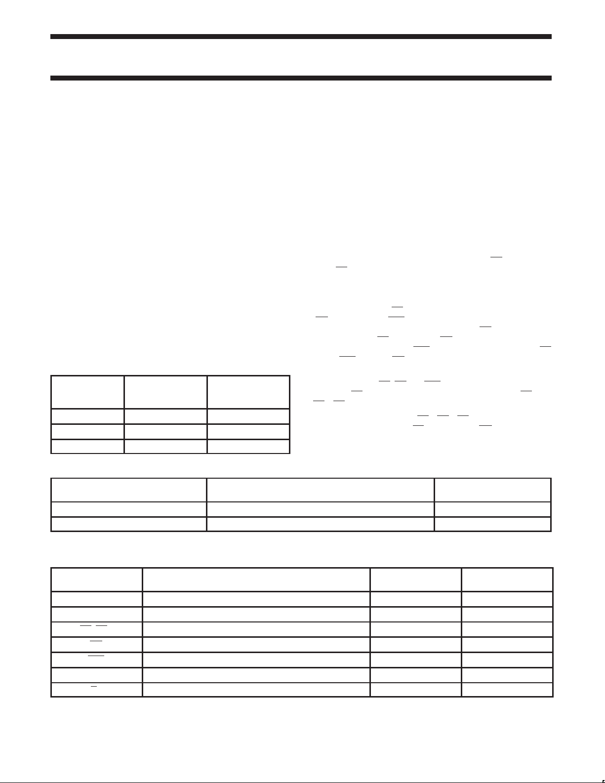
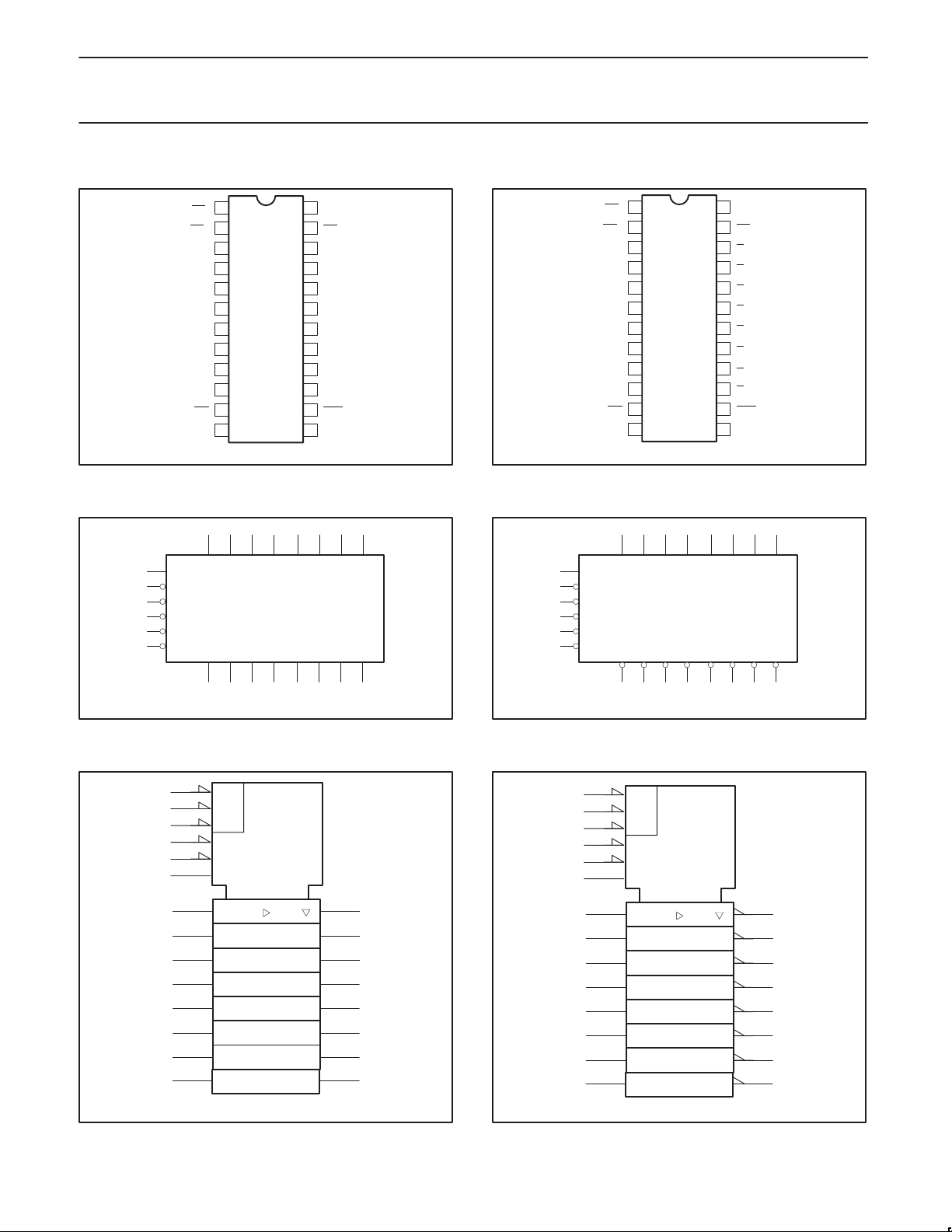
PIN CONFIGURATION for 74F841
1
OE
2
D0
3
D1
4
D2
5
D3
6
D4
7
D5
8
D6
9
D7
10
D8
11
D9
GND
12 13
LOGIC SYMBOL for 74F841
24
23
22
21
20
19
18
17
16
15
14
SF01279
V
Q0
Q1
Q2
Q3
Q4
Q5
Q6
Q7
Q8
Q9
LE
74F841/74F842/74F843/
74F845/74F846
PIN CONFIGURATION for 74F842
1
CC
OE
2
D0
3
D1
4
D2
5
D3
6
D4
7
D5
8
D6
9
D7
10
D8
11
D9
12 13
GND
LOGIC SYMBOL for 74F842
24
23
22
21
20
19
18
17
16
15
14
SF01282
V
CC
Q0
Q
1
Q
2
Q
3
4
Q
Q
5
Q6
7
Q
Q
8
Q
9
LE
3456 78910
2
D0LED1 D2 D3 D4 D5 D6 D7 D8
13
1
OE
Q0 Q1 Q2 Q3 Q4 Q5 Q6 Q7 Q8 Q9
= Pin 24
V
CC
GND = Pin 12
23 22 21 20 19 18 17 16 15 14
LOGIC SYMBOL (IEEE/IEC) for 74F841
1
EN
13
C1
1 D
4
5
6
7
8
9
10
SF01280
232
223
21
20
19
18
17
16
15
1411
11
D9
13
1
= Pin 24
V
CC
GND = Pin 12
3456 78910
2
D0LED1 D2 D3 D4 D5 D6 D7 D8
OE
Q0 Q1 Q2 Q3 Q4 Q5 Q6 Q7 Q8 Q9
23 22 21 20 19 18 17 16 15 14
11
D9
SF01283
LOGIC SYMBOL (IEEE/IEC) for 74F842
1
EN
13
C1
1 D
4
5
6
7
8
9
10
11
232
223
21
20
19
18
17
16
15
14
1999 Jun 23
SF01281
SF01284
3
Philips Semiconductors Product specification
Bus interface latches
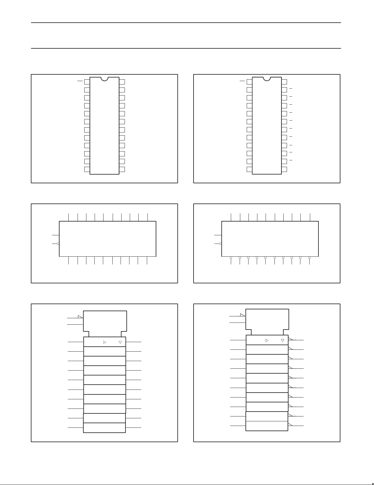
PIN CONFIGURATION for 74F843
1
OE
2
D0
3
D1
4
D2
5
D3
6
D4
7
D5
8
D6
9
D7
10
D8
11
MR
12 13
GND
LOGIC SYMBOL for 74F843
24
23
22
21
20
19
18
17
16
15
14
SF01285
V
CC
Q0
Q1
Q2
Q3
Q4
Q5
Q6
Q7
Q8
PRE
LE
74F841/74F842/74F843/
74F845/74F846
3456 78910
2
13
14 PRE
11 MR
1OE
= Pin 24
V
CC
GND = Pin 12
D0LED1 D2 D3 D4 D5 D6 D7 D8
Q0 Q1 Q2 Q3 Q4 Q5 Q6 Q7 Q8
23 22 21 20 19 18 17 16 15
LOGIC SYMBOL (IEEE/IEC) for 74F843
1
EN
11
R
14
S2
13
C1
1 D
4
5
6
7
8
9
10
SF01286
232
223
21
20
19
18
17
16
15
1999 Jun 23
SF01287
4
Philips Semiconductors Product specification
Bus interface latches
PIN CONFIGURATION for 74F845
1
OE
0
2
1
OE
3
D0
4
D1
5
D2
6
D3
7
D4
8
D5
9
D6
10
D7
11
MR
12 13
GND
LOGIC SYMBOL for 74F845
3456 78910
24
23
22
21
20
19
18
17
16
15
14
SF01291
V
CC
OE2
Q0
Q1
Q2
Q3
Q4
Q5
Q6
Q7
PRE
LE
74F841/74F842/74F843/
74F845/74F846
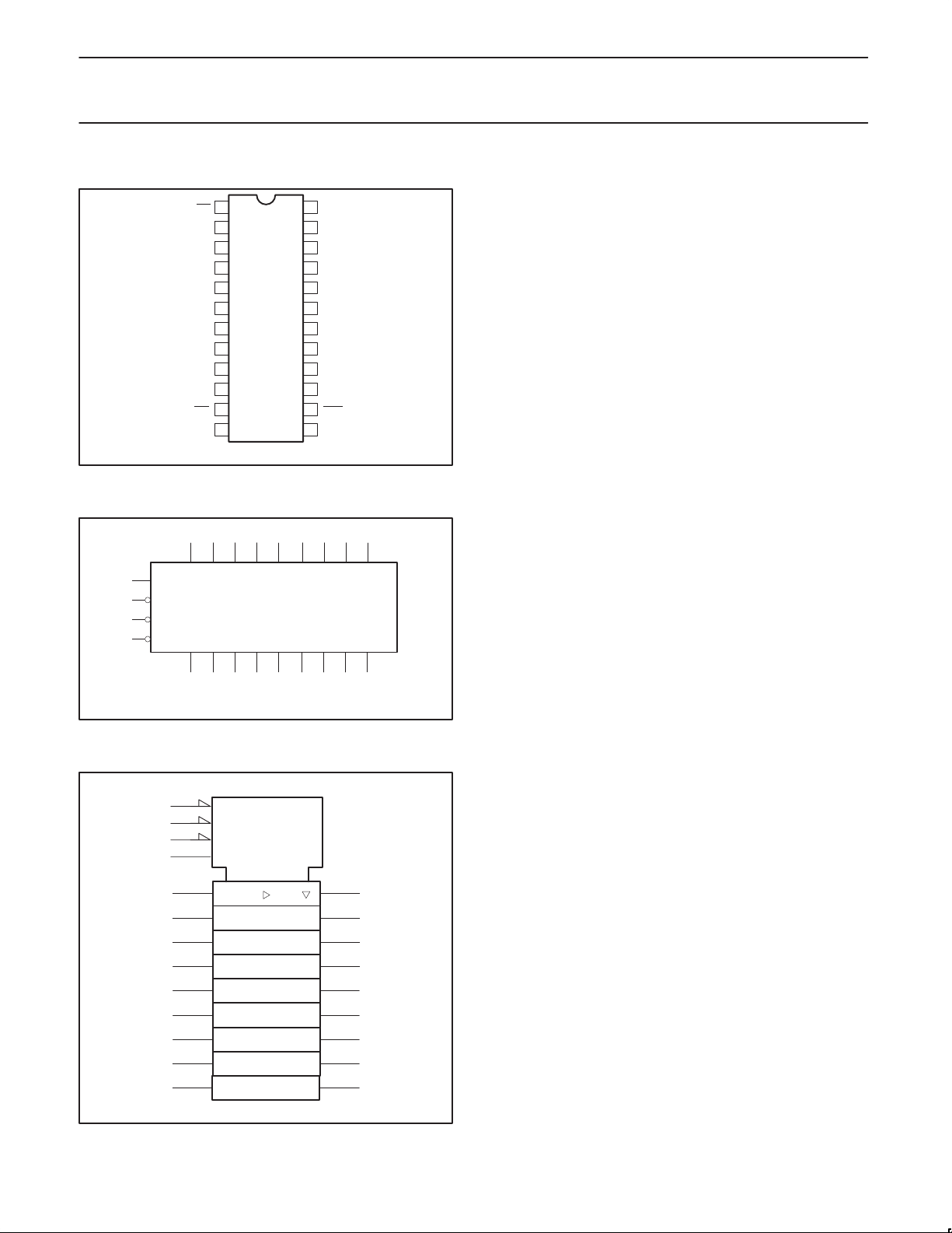
PIN CONFIGURATION for 74F846
1
OE
0
2
1
OE
3
D0
4
D1
5
D2
6
D3
7
D4
8
D5
9
D6
10
D7
11
MR
12 13
GND
LOGIC SYMBOL for 74F846
3456 78910
24
23
22
21
20
19
18
17
16
15
14
SF01294
V
OE2
Q
Q
Q
Q
Q
Q
Q
Q
PRE
LE
CC
0
1
2
3
4
5
6
7
13
14 PRE
11 MR
1 OE0
2 OE1
23 OE2
V
= Pin 24
CC
GND = Pin 12
D0LED1 D2 D3 D4 D5 D6 D7
Q0 Q1 Q2 Q3 Q4 Q5 Q6 Q7
22 21 20 19 18 17 16 15
SF01292
LOGIC SYMBOL (IEEE/IEC) for 74F845
1
&
2
23
14
11
13
4
5
6
7
8
9
10
EN
S2
R
C1
1 D
13
14 PRE
11 MR
1 OE0
2 OE1
23 OE2
V
= Pin 24
CC
GND = Pin 12
D0LED1 D2 D3 D4 D5 D6 D7
Q0 Q1 Q2 Q3 Q4 Q5 Q6 Q7
22 21 20 19 18 17 16 15
SF01295
LOGIC SYMBOL (IEEE/IEC) for 74F846
1
&
2
23
14
11
13
223
21
20
19
18
17
16
15
4
5
6
7
8
9
10
S2
R
C1
1 D
EN
223
21
20
19
18
17
16
15
1999 Jun 23
SF01293A
SF01296A
5
Philips Semiconductors Product specification
INPUTS
Transparent
Latched
Bus interface latches
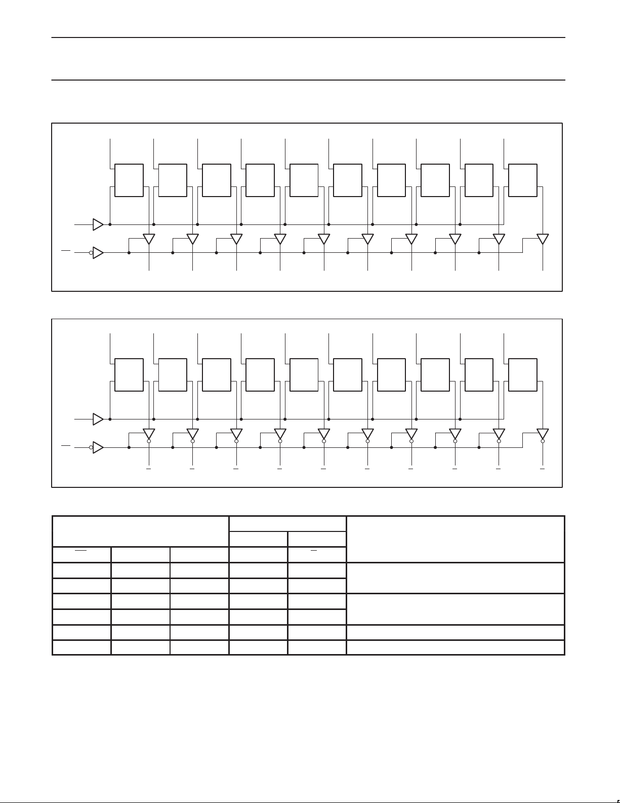
LOGIC DIAGRAM for 74F841
D0
2
D
LQ
13
LE
1
OE
VCC = Pin 24
GND = Pin 12
LOGIC DIAGRAM for 74F842
D0
2
D1
3
D
LQ
23
Q0
D1
3
D2
4
22
Q1
D2
4
D
LQ
Q2
D3
5
D
LQ
21
D3
5
D4
6
20
Q3
D4
6
D
LQ
Q4
D5
7
D
LQ
19
D5
7
D6
8
18
Q5
D6
8
74F841/74F842/74F843/
74F845/74F846
D
LQ
C
Q6
D7
9
D
LQ
17
D7
9
D8
10
16
Q7
D8
10
D9
11
D
LQ
15
Q8
D9
11
D
LQ
14
Q9
SF01297
13
LE
1
OE
VCC = Pin 24
GND = Pin 12
D
LQ
23
Q0
D
LQ
Q1
D
LQ
22
21
Q2
D
LQ
Q3
D
LQ
20
D
LQ
19
Q4
FUNCTION TABLE for 74F841 and 74F842
OUTPUTS
74F841 74F842
OE LE Dn Qn Qn
L H L L H
L H H H L
L ↓ l L H
L ↓ h H L
H X X Z Z High Impedance
L L X NC NC Hold
H = High voltage level
L = Low voltage level
h = High state one setup time before the High-to-Low LE transition
l = Low state one setup time before the High-to-Low LE transition
↓ = High-to-Low transition
X = Don’t care
NC= No change
Z = High impedance “off” state
18
Q5
p
D
LQ
C
Q6
D
LQ
17
D
LQ
16
Q7
OPERATING MODE
15
Q8
D
LQ
14
Q9
SF01298
1999 Jun 23
6
 Loading...