

Philips 74f835 DATASHEETS
Philips Semiconductors
Product specification
74F835
8-bit shift register with 2:1 mux-in,
latched “B” inputs, and serial out
1
1990 Jan 08 853–0615 99490
FEATURES
•Specifically designed for Video applications
•Combines the 74F373, two 74F157s, and the 74F166 functions in
one package
•Interleaved loading with 2:1 mux
•Dual 8-bit parallel inputs
•Transparent latch on all “B” inputs
•Guaranteed serial shift frequency to 100MHz
•Expandable to 16-bits or more with serial input
DESCRIPTION
The 74F835 is a high speed 8-bit parallel/serial-in, serial-out shift
register whose parallel inputs have been connected to an internal
octal two-to-one multiplexer with all the “B” inputs connected to an
octal latch.
This 24-pin part is specifically designed for video bit shifting, where
interleaved loading is desired and parts count is critical. It is useful in
any design where a 2:1 mux input with a transparent latch is
needed.
TYPE
TYPICAL f
MAX
TYPICAL
SUPPLY CURRENT
(TOTAL)
74F835 150MHz 45mA
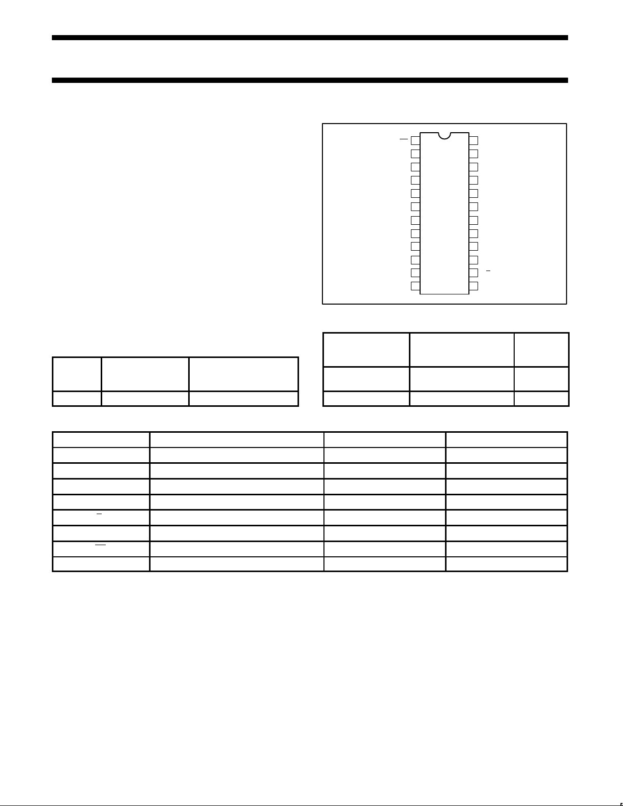
PIN CONFIGURATION
1
2
3
4
5
6
7
8
9
10
11
12 13
14
15
16
17
18
19
20
21
22
23
24
PE
CP
D4A
D4B
D5A
D5B
D6A
D6B
D7A
D7B
Q7
V
CC
D3B
D3A
D2B
D2A
D1B
D1A
D0A
D0B
DS
SA
/B
LE
GND
SF01355
ORDERING INFORMATION
DESCRIPTION
COMMERCIAL RANGE
V
CC
= 5V ±10%,
T
amb
= 0°C to +70°C
PACKAGE
DRAWING
NUMBER
24-pin plastic
Slim DIP (300 mil)
N74F835N SOT222-1
24-pin plastic SOL N74F835D SOT137-1
INPUT AND OUTPUT LOADING AND FAN-OUT TABLE
PINS DESCRIPTION 74F (U.L.) HIGH/LOW LOAD VALUE HIGH/LOW
D0A – D7A Parallel data inputs 1.0/1.0 20µA/0.6mA
D0B – D7B Latched Parallel data inputs 1.0/1.0 20µA/0.6mA
DS Serial data input 1.0/1.0 20µA/0.6mA
CP Shift Register Clock input (active rising edge) 1.0/1.0 20µA/0.6mA
SA/B Mux Select 1.0/1.0 20µA/0.6mA
LE Latch Enable input (for B inputs) 1.0/1.0 20µA/0.6mA
PE Parallel Enable input 1.0/1.0 20µA/0.6mA
Q7 Output 50/33 1.0mA/20mA
NOTE: One (1.0) FAST unit load is defined as: 20µA in the High state and 0.6mA in the Low state.

Philips Semiconductors Product specification
74F835
8-bit shift register with 2:1 mux-in,
latched “B” inputs, and serial out
1990 Jan 08
2
LOGIC SYMBOL
2
1
13
14
CP
PE
LE
SA
/B
15 16 17 18 19 20 21 22 23 3 4 5 6 7 8 9 10
11
Q7
DS
D0A
D0B
D1A
D1B
VCC = PIN 24
GND = PIN 12
SF01356
D2A
D2B
D3A
D3B
D4A
D4B
D5A
D5B
D6A
D6B
D7A
D7B
IEC/IEEE SYMBOL
SF01357
2
C1
SRG 8
MUX
1
M4
13
EN3
14
G2
15
1,4
16
1, 2
, 3, 4
17
1, 2, 3, 4
18
19
20
21
22
23
3
4
5
6
7
8
9
10
11
TYPICAL TIMING DIAGRAM
SET B
UNLOAD
B LATCH
SHIFT BSHIFT A
LOAD A
LOAD B LATCH
PE
CP
LE
SA
/B
D0A
D7A
D0B
D7B
Q7
q7A q6A q1A q0A q7B q6B q5B q0B
SF01359
 Loading...