Philips 74f777 DATASHEETS

INTEGRATED CIRCUITS
74F777
Triple bidirectional latched bus
transceiver (3-State + open collector)
Product specification
IC15 Data Handbook
1992 May 19

Philips Semiconductors Product specification
Triple bidirectional latched bus transceiver (3–State +
Open Collector)
FEA TURES
•Latching transceiver
•High drive Open Collector output current with minimum output
swing
•Compatible with Test Mode (TM) bus specification
•Controlled output ramp
•Multiple package options
•Industrial temperature range available (–40°C to +85°C)
DESCRIPTION
The 74F777 is a triple bidirectional latched bus transceiver and is
intended to provide the electrical interface to a high performance
wired–OR bus. This bus has a loaded characteristics impedance
ORDERING INFORMATION
DESCRIPTION COMMERCIAL RANGE INDUSTRIAL RANGE PKG DWG #
VCC = 5V ±10%, T
20–pin plastic DIP (300 mil) N74F777N I74F777N SOT146-1
20–pin PLCC N74F777A I74F777A SOT380-1
= 0°C to +70°C
amb
range of 20 to 50 ohms and is terminated on each end with a 30 to
40 ohm resistor.
The 74F777 is a triple bidirectional transceiver with Open Collector
B and 3–State A port output drivers. A latch function is provided for
the A port signals. The B port output driver is designed to sink
100mA from 2 volts to minimize crosstalk and ringing on the bus.
A separate output threshold clamp voltage (V
prevent the A port output High level from exceeding future high
density processor supply voltage levels. For 5 volt systems, V
simply tied to V
TYPE TYPICAL
74F777 7.0ns 45mA
ORDER CODE
CC.
PROPAGATION DELAY
VCC = 5V ±10%,
T
= –40°C to +85°C
amb
TYPICAL SUPPL Y CUR-
74F777
) is provided to
X
RENT( TOTAL)
is
X
INPUT AND OUTPUT LOADING AND FAN OUT TABLE
PINS DESCRIPTION 74F (U.L.)
A0 – A2 PNP latched inputs 3.5/0.1 17 70µA/70µA
B0 – B2 Data inputs with threshold circuitry 5.0/0.167
OEA0 – OEA2 A output enable inputs (active–High) 1.0/0.033
OEB0 – OEB2 B output enable inputs (active–Low) 1.0/0.033
LE0 – LE2 Latch enable inputs (active–Low) 1.0/0.033
A0 – A2 3–State outputs 150/40 3mA/24mA
B0 – B2 Open Collector outputs OC/166.7 OC/100mA
Note to input and output loading and fan out table
One (1.0) FAST unit load is defined as: 20µA in the High state and 0.6mA in the Low state.
OC = Open Collector.
HIGH/LOW
LOAD VALUE
HIGH/LOW
100µA/100µA
20µA/20µA
20µA/20µA
20µA/20µA
May 19, 1992 853–1645 06772
2

Philips Semiconductors Product specification
Triple bidirectional latched bus transceiver (3–State +
Open Collector)
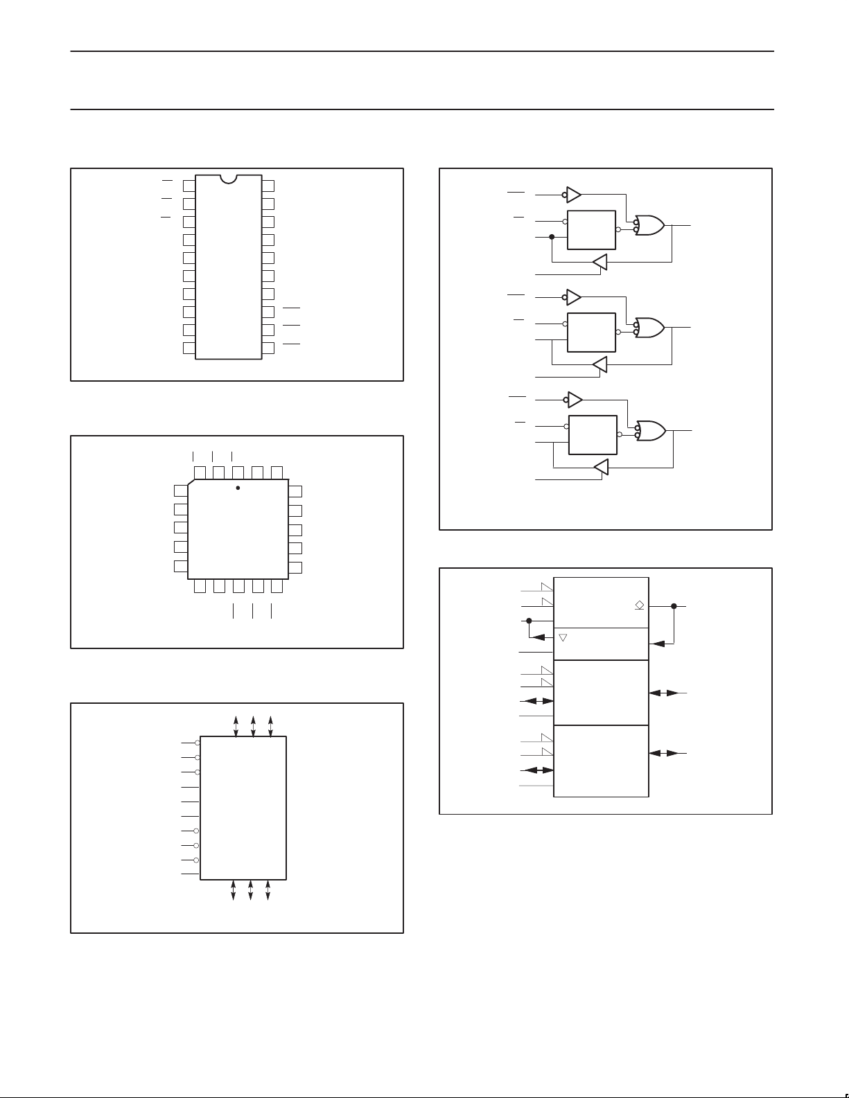
PIN CONFIGURATION
LE
0
1
1
LE
2
LE2
3
OEA0
4
A0
5
OEA1
6
A1
7
OEA2
8
A2
9
10 11
GND
PIN CONFIGURA TION PLCC
LE1
LE0
LE2
3212019
4
OEA0
5
A0
OEA1
OEA2
6
7
A1
8
PLCC
A2
GND
OEB2
LOGIC SYMBOL
5 7 9
20
19
18
17
16
15
14
13
12
SF00432
Vcc
131211109
OEB1
V
CC
V
X
GND
B0
B1
B2
GND
OEB
OEB
OEB
Vx
18
17
16
15
14
OEB0
SF00433
0
1
2
GND
B0
B1
B2
GND
LOGIC DIAGRAM
= Pin 20, VX = Pin 19,
V
CC
GND = Pin 10, 14, 18
IEC/IEEE SYMBOL
OEB
LE0
A0
OEA0
OEB
LE1
A1
OEA1
OEB
LE2
A2
OEA2
74F777
13
0
1
LE
5
4
12
1
2
7
6
11
2
3
9
8
13
EN
1
C1
5
4
EN
12
2
7
6
Q
Data
LE
Q
Data
LE
Q
Data
ID
17
16
15
SF00436
17
16
B0
B1
B2
V
= Pin 20, V
CC
GND = Pin 10, 14, 18
May 19, 1992
13
12
11 OEB2
19
= Pin 19,
X
LE0
LE1
LE2
OEA0
OEA1
OEA2
OEB0
OEB1
V
X
A0 A1 A2
B0 B1 B2
17 16 15
SF00434
1
2
3
4
6
8
11
3
9
8
15
SF00435
3

Philips Semiconductors Product specification
Triple bidirectional latched bus transceiver (3–State +
Open Collector)
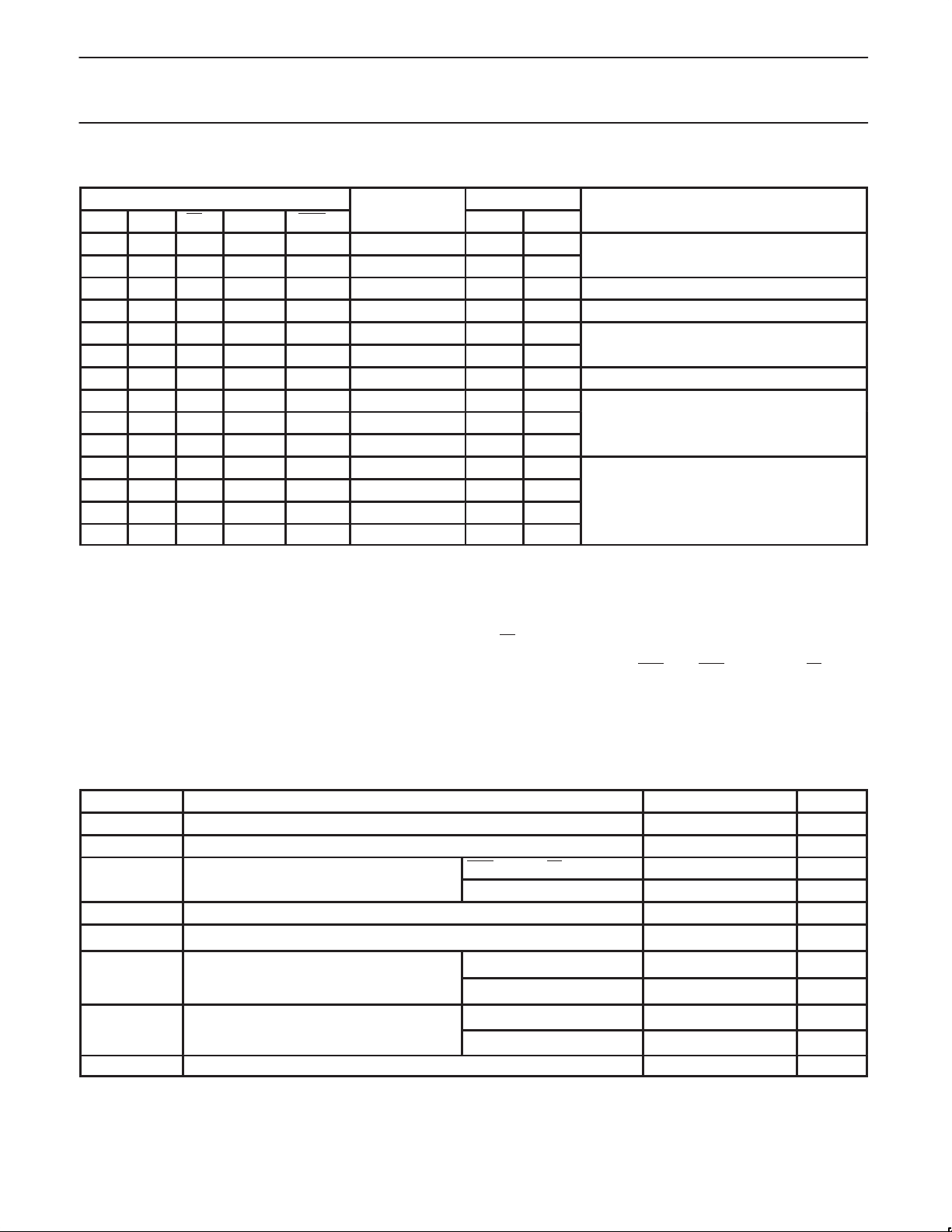
FUNCTION TABLE
INPUTS LATCH OUTPUTS OPERATING MODE
An Bn* LEn OEAn OEBn STATE An Bn
H X L L L H Z H** A 3-State, data from A to B
L X L L L L Z L
X X H L L Qn Z Qn A 3-State, latched data to B
– – L H L (1) (1) (1) Feedback: A to B, B to A
– H H H L H (2) H Z(2) Preconditioned latch enabling
– L H H L H (2) L Z(2) data transfer from B to A
– – H H L Qn Qn Qn Latch state to A and B
H X L L H H Z Z
L X L L H L Z Z B and A 3–State
X X H L H Qn Z Z
– H L H H H H Z
– L L H H L L Z B 3-State, data from B to A
– H H H H Qn H Z
– L H H H Qn
Notes to function table
H = High voltage level
L = Low voltage level
X = Don’t care
– = Input not externally driven
Z = High impedance (off) state
Q
= High or Low voltage level one setup time prior to the Low–to–High LE transition.
n
(1) = Condition will cause a feedback loop path: A to B and B to A.
(2) = The latch must be preconditioned such that B inputs may assume a High or Low level while OEB
* =Precaution should be taken to insure the B inputs do not float. If they do they are equal to Low state.
B
n
H**= Goes to level of pull-up voltage.
Each latch is independent. The latches may be run in any combination of modes.
Qn
L Z
0 and OEB1 are Low and LE is High.
74F777
ABSOLUTE MAXIMUM RATINGS
(Operation beyond the limit set forth in this table may impair the useful life of the device. Unless otherwise noted these limits are over the
operating free air temperature range.)
SYMBOL PARAMETER RATING UNIT
V
V
V
I
IN
V
I
OUT
T
T
CC
X
IN
OUT
amb
stg
Supply voltage –0.5 to +7.0 V
Threshold control –0.5 to +7.0 V
Input voltage OEBn, OEAn, LEn –0.5 to +7.0 V
A0 – A2, B0 – B2 –0.5 to +5.5 V
Input current –30 to +5 mA
Voltage applied to output in High output state –0.5 to V
Current applied to output in A0 – A2 48 mA
Low output state B0 – B2 200 mA
Operating free air Commercial range 0 to +70
temperature range Industrial range –40 to +85
Storage temperature range –65 to +150
CC
V
°C
°C
°C
May 19, 1992
4
 Loading...