

Philips 74f651 a, 74f652 a DATASHEETS
INTEGRATED CIRCUITS
74F651A/74F652A
Transceivers/registers
Product specification
Replaces datasheet 74F651/74F652/74F651A/74F652A of 1990 Oct 23
IC15 Data Handbook
1999 Jun 23
Philips Semiconductors Product specification
DESCRIPTION
PKG DWG #
74F651A/74F652AT ransceivers/registers
74F651A Octal transceiver/register, inverting (3-State)
74F652A Octal transceiver/register, non-inverting (3-State)
FEA TURES
•Combines 74F245 and two 74F374 type functions in one chip
•High impedance base inputs for reduced loading (70µA in high
and low states)
•Independent registers for A and B buses
•Multiplexed real-time and stored data
DESCRIPTION
The 74F651A and 74F652A transceivers/registers consist of bus
transceiver circuits with 3–State outputs, D–type flip–flops, and
control circuitry arranged for multiplexed transmission of data
directly from the input bus or the internal registers. Data on the A or
B bus will be clocked into the registers as the appropriate clock pin
goes high. Output enable (OEAB, OEBA
pins are provided for bus management.
•Choice of non-inverting and inverting data paths
•3-State outputs
•Industrial temperature range available (–40°C to +85°C) for
74F652A
TYPE
74F651/74F652 110MHz 140mA
74F651A/74F652A 175MHz 110mA
ORDERING INFORMATION
24–pin plastic slim DIP (300mil) N74F651AN, N74F652AN I74F652AN SOT222-1
24–pin plastic SOL N74F651AD, N74F652AD I74F652AD SOT137-1
TYPICAL f
max
ORDER CODE
COMMERCIAL RANGE INDUSTRIAL RANGE
VCC = 5V ±10%, VCC = 5V ±10%,
T
= 0°C to +70°C T
amb
TYPICAL SUPPLY CURRENT( TOTAL)
= –40°C to +85°C
amb
) and select (SAB, SBA)
INPUT AND OUTPUT LOADING AND FAN OUT TABLE
PINS DESCRIPTION 74F (U.L.) HIGH/LOW LOAD VALUE HIGH/LOW
A0 – A7, B0 – B7 A, B inputs 3.5/0.1 16 70µA/70µA
CPAB, CPBA A–to–B, B–to–A clock inputs 1.0/0.033 20µA/20µA
SAB, SBA A–to–B, B–to–A select inputs 1.0/0.033 20µA/20µA
OEAB, OEBA A–to–B, B–to–A output enable inputs 1.0/0.033 20µA/20µA
A0 – A7, B0 – B7 A, B outputs for N74F651, N74F652 750/106.7 15mA/64mA
A0 – A7, B0 – B7 A, B outputs for N74F651A, N74F652A 750/80 15mA/48mA
A0 – A7, B0 – B7 A, B outputs for I74F652A 750/60 15mA/36mA
Note to input and output loading and fan out table
1. One (1.0) FAST unit load is defined as: 20µA in the high state and 0.6mA in the low state.
1999 Jun 23 853–1 126 21852
2
Philips Semiconductors Product specification
74F651A/74F652ATransceivers/registers
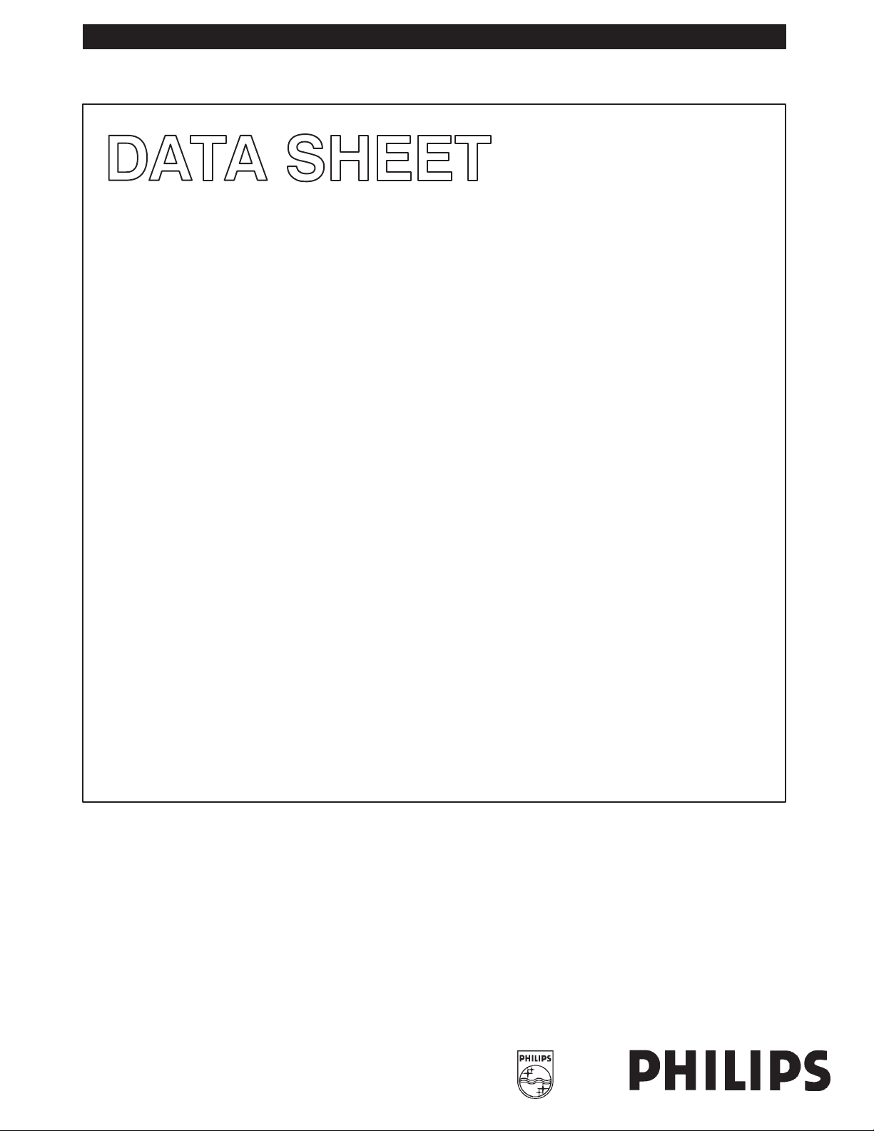
PIN CONFIGURATION
1
CPAB
2
SAB
3
OEAB
4
A0
5
A1
6
A2
7
A3
A4
8
A5
9
A6
10
A7
11
GND
IEC/IEEE SYMBOL
21
3
23
22
1
2
4
5
6
7
8
9
10
11
EN1 [BA]
EN1 [AB]
G3
G5
C6
G7
1
6D
74F651A
74F651A
1
7
1
7
LOGIC SYMBOL
74F651A
24
V
23
22
21
20
19
18
17
16
15
14
1312
SF00401
CC
CPBA
SBA
OEBA
B0
B1
B2
B3
B4
B5
B6
B7
= Pin 24
V
CC
GND = Pin 12
4567891011
A0 A1 A2 A3 A4 A5 A6 A7
CPAB
1
SAB
2
OEAB
3
CPBA
23
SBA
22
OEBA
21
B0 B1 B2 B3 B4 B5 B6 B7
20 19 18 17 16 15 14 13
SF00402
LOGIC DIAGRAM
21
OEBA
3
OEAB
23
CPBA
22
SBA
1
CPAB
2
SAB
I of 8 channels
5
4D
1
5
1
2
20
4
A0
19
18
17
16
15
14
13
1D
C1
74F651A
1D
C1
20
B0
1999 Jun 23
SF00403
3
VCC = Pin 24
GND = Pin 12
to 7 other channels
SF00404
Philips Semiconductors Product specification
74F651A/74F652ATransceivers/registers
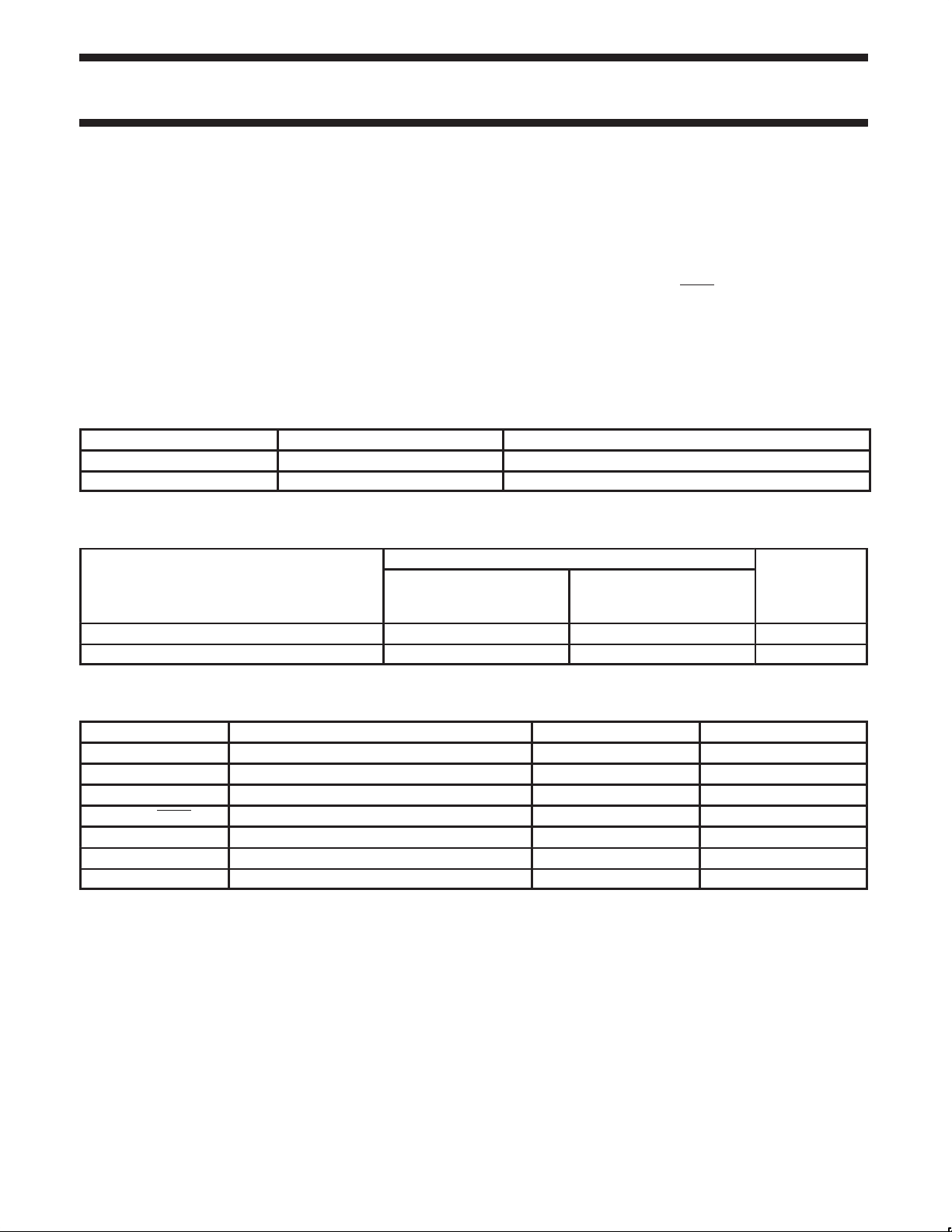
PIN CONFIGURATION
1
CPAB
2
SAB
3
OEAB
4
A0
5
A1
6
A2
7
A3
A4
8
A5
9
A6
10
A7
11
GND
IEC/IEEE SYMBOL
21
3
23
22
1
2
4
5
6
7
8
9
10
11
EN1 [BA]
EN1 [AB]
G3
G5
C6
G7
1
6D
74F652A
74F652A
1
7
1
7
LOGIC SYMBOL
74F652A
24
V
23
22
21
20
19
18
17
16
15
14
1312
SF00405
CC
CPBA
SBA
OEBA
B0
B1
B2
B3
B4
B5
B6
B7
= Pin 24
V
CC
GND = Pin 12
4567891011
A0 A1 A2 A3 A4 A5 A6 A7
CPAB
1
SAB
2
OEAB
3
CPBA
23
SBA
22
OEBA
21
B0 B1 B2 B3 B4 B5 B6 B7
20 19 18 17 16 15 14 13
SF00406
LOGIC DIAGRAM
21
OEBA
3
OEAB
23
CPBA
22
SBA
1
CPAB
2
SAB
I of 8 channels
5
4D
1
5
1
2
20
4
A0
19
18
17
16
15
14
13
74F652A
1D
C1
20
1D
C1
B0
1999 Jun 23
SF00407
to 7 other channels
SF00408
4
Philips Semiconductors Product specification
74F651A/74F652ATransceivers/registers
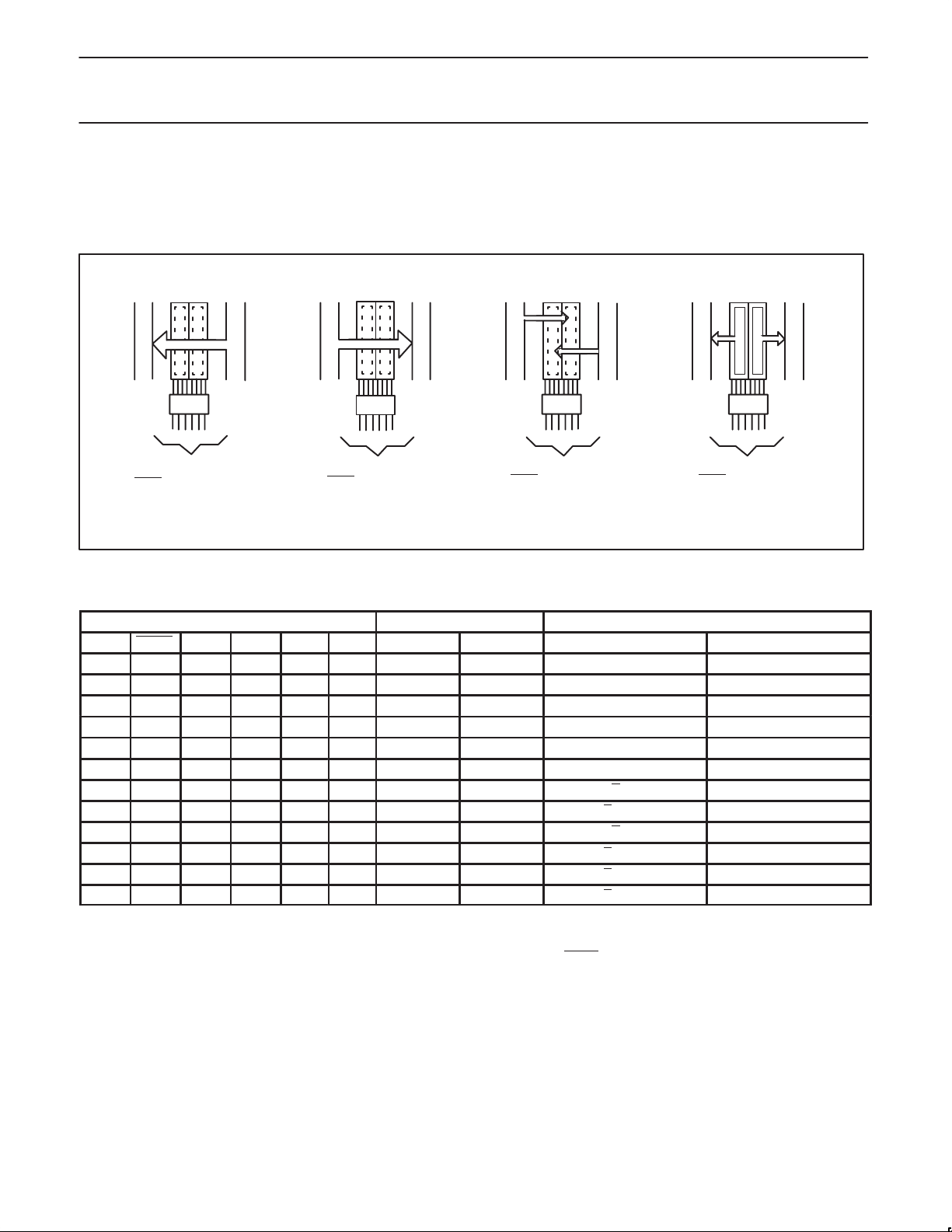
The following examples demonstrate the four fundamental
bus-management functions that can be performed with the 74F651A
transferred through the device in real time. The output enable pins
determine the direction of the data flow.
and 74F652A. The select pins determine whether data is stored or
BUS MANAGEMENT FUNCTIONS
REAL TIME BUS TRANSFER
BUS A
OEAB OEBA CPAB CPBA SAB SBA
L LX XXL HHXXLX XH↑ XXX
BUS B TO BUS A
BUS B
REAL TIME BUS TRANSFER
BUS A TO BUS B
BUS A BUS A
OEAB OEBA
CPAB CPBA SAB SBA
STORAGE FROM
A, B, OR A AND B
OEAB OEBA
LXX↑ XX
LH↑↑XX
CPAB CPBA SAB SBA OEAB OEBA CPAB CPBA SAB SBA
TRANSFER STORED DATA
TO A AND/OR B
BUS A BUS BBUS BBUS B
H L H or L H or L H H
SF00409
FUNCTION TABLE
INPUTS DATA I/O OPERATING MODE
OEAB OEBA CPAB CPBA SAB SBA An Bn 74F651A 74F652A
L H H or L H or L X X Input Input Isolation Isolation
L H ↑ ↑ X X Input Input Store A and B data Store A and B data
X H ↑ H or L X X Input Unspecified* Store A, hold B Store A hold B
H H ↑ ↑ L X Input Output Store A in both registers Store A in both registers
L X H or L ↑ X X Unspecified* Input Hold A, store B Hold A, store B
L L ↑ ↑ X L Output Input Store B in both registers Store B in both registers
L L X X X L Output Input Real time B data to A bus Real time B data to A bus
L L X H or L X H Output Input Stored B data to A bus Stored B data to A bus
H H X X L X Input Output Real time A data to B bus Real time A data to B bus
H H H or L X H X Input Output Stored A data to B bus Stored A data to B bus
H L H or L H or L H H Output Output Stored A data to B bus Stored A data to B bus
H L H or L H or L H H Output Output Stored B data to A bus Stored B data to A bus
Notes to function table
1. H = High-voltage level
2. L = Low-voltage level
3. * = The data output function may be enabled or disabled by various signals at the OEBA
always enabled, i.e., data at the bus pins will be stored on every low-to-high transition of the clock.
4. ↑ = Low-to-high clock transition
5. X = Don’t care
and OEAB inputs. Data input functions are
1999 Jun 23
5
 Loading...