

Philips 74f647, 74f649 DATASHEETS

INTEGRATED CIRCUITS
74F647
Octal transceiver/register, non-inverting
(open-collector)
74F649
Octal transceiver/register, inverting
(open-collector)
Product specification
IC15 Data Handbook
1992 Feb 28
Philips Semiconductors Product specification
74F647/74F649Octal transceivers/registers (open-collector)
74F647 Octal Transceiver/Register, Non-inverting (Open Collector)
74F649 Octal Transceiver/Register, Inverting (Open Collector)
FEA TURES
•High impedance NPN base inputs for reduced loading
(20µA in High and Low states)
•Independent registers for A and B buses
•Multiplexed real-time and stored data
•Choice of non-inverting and inverting data paths
•Open Collector outputs
•300 mil wide 24-pin Slim Dip package
DESCRIPTION
The 74F647 and 74F649 Transceivers/Registers consist of bus
transceiver circuits with open-collector outputs, D-type flip-flops, and
control circuitry arranged for multiplexed transmission of data
directly from the input bus or from the internal registers. Data on the
A or B bus will be clocked into the registers as the appropriate clock
pin goes to a High logic level. Output Enable (OE
provided to control the transceiver function. In the transceiver mode,
data present at the high impedance port may be stored in either the
A or B register or both.
The select (SAB, SBA) controls can multiplex stored and real-time
(transparent mode) data. The DIR determines which bus will receive
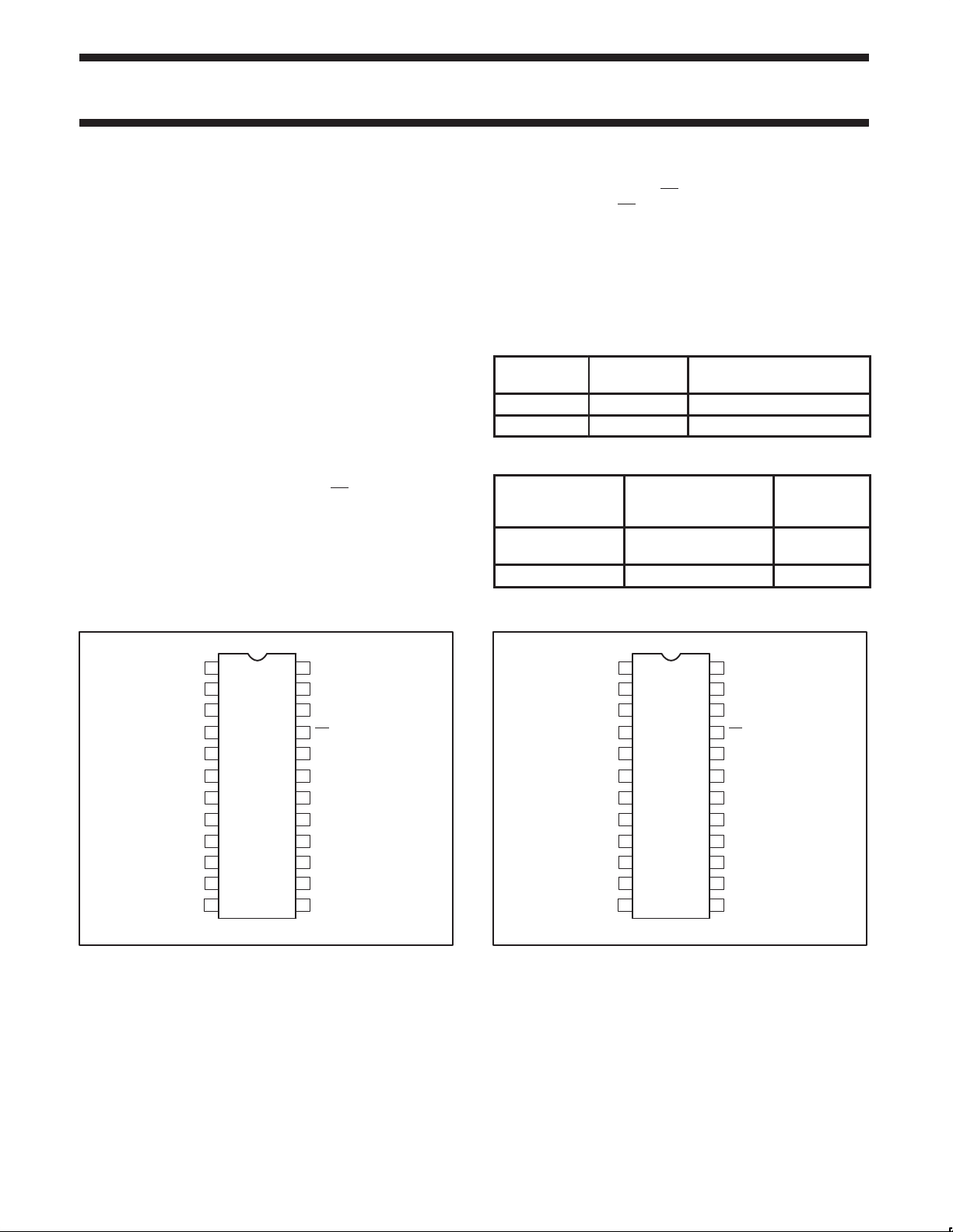
PIN CONFIGURATION – 74F647
) and DIR pins are
data when the Output Enable, OE
mode (Output Enable, OE
is active Low. In the isolation
= High), data from Bus A may be stored
in the B register and/or data from Bus B may be stored in the A
register.
When an output function is disabled, the input function is still
enabled and may be used to store and transmit data. Only one of
the two buses, A or B, may be driven at a time. The following
examples demonstrate the four fundamental bus-management
functions that can be performed with the 74F647 and 74F649.
TYPE
TYPICAL
f
max
TYPICAL SUPPL Y CURRENT
(TOTAL)
74F647 65MHz 125mA
74F649 65MHz 125mA
ORDERING INFORMATION
COMMERCIAL RANGE
DESCRIPTION
24-pin plastic Slim
VCC = 5V ±10%,
T
= 0°C to +70°C
amb
PKG DWG #
N74F647N, N74F649N SOT222-1
DIP (300mil)
24-pin plastic SOL N74F647D, N74F649D SOT137-1
PIN CONFIGURATION – 74F649
CPAB
SAB
DIR
GND
1
2
3
4
A0
5
A1
6
A2
7
A3
8
A4
9
A5
10
A6
11
A7
24
23
22
21
20
19
18
17
16
15
14
1312
SF01196
V
CC
CPBA
SBA
OE
B0
B1
B2
B3
B4
B5
B6
B7
CPAB
SAB
DIR
GND
1
2
3
4
A0
5
A1
6
A2
7
A3
8
A4
9
A5
10
A6
11
A7
24
23
22
21
20
19
18
17
16
15
14
1312
SF01196
V
CC
CPBA
SBA
OE
B0
B1
B2
B3
B4
B5
B6
B7
1992 Feb 28 853-0876 05853
2
Philips Semiconductors Product specification
74F647/74F649Octal transceivers/registers (open-collector)
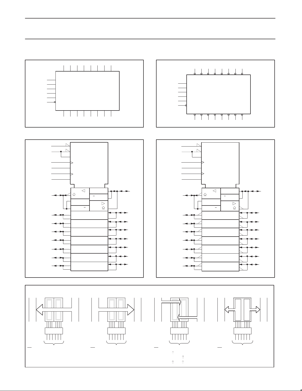
LOGIC SYMBOL – 74F647
4567891011
A0 A1 A2 A3 A4 A5 A6 A7
CPAB
1
SAB
2
DIR
3
CPBA
SBA
OE
B0 B1 B2 B3 B4 B5 B6 B7
20 19 18 17 16 15 14 13
VCC=Pin 24
GND=Pin 12
23
22
21
LOGIC SYMBOL – 74F647
21
3
23
22
1
2
4
5
6
7
8
9
10
11
G3
3EN1(BA)
3EN2(AB)
C4
G5
C6
G7
1
≥
1
6D
1
LOGIC SYMBOL – 74F649
4567891011
A0 A1 A2 A3 A4 A5 A6 A7
CPAB
1
SAB
2
DIR
3
CPBA
SBA
OE
B0 B1 B2 B3 B4 B5 B6 B7
20 19 18 17 16 15 14 13
SF01198
SF01197
VCC=Pin 24
GND=Pin 12
23
22
21
LOGIC SYMBOL – 74F648
21
3
23
22
1
2
4D
5
1
5
7
≥ 1
2
7
20
19
18
17
16
15
14
13
4
5
6
7
8
9
10
11
G3
3EN1(BA)
3EN2(AB)
C4
G5
C6
G7
1
≥
1
6D
1
4D
5
1
5
7
≥ 1
2
7
20
19
18
17
16
15
14
13
SF01199
REAL TIME BUS TRANSFER
BUS B TO BUS A
BUS A BUS B BUS A BUS B BUS A BUS B BUS A BUS B
OE
DIRLCPABXCPBAXSABXSBA
L
L
1992 Feb 28
REAL TIME BUS TRANSFER
BUS A TO BUS B
OELDIRHCPABXCPBAXSABLSBA
X
OE
DIR
X
X
H
STORAGE FROM
A, B, OR A AND B
CPABXCPBAXSAB
X
X
X
SBA
X
X
X
X
X
X
TRANSFER STORED DATA
DIR
OE
L
L
L
H
3
TO A OR B
CPAB
X
HorL
SF01200
CPBA
H or L
X
SAB
X
H
SF01201
SBA
H
X
Philips Semiconductors Product specification
74F647/74F649Octal transceivers/registers (open-collector)
INPUT AND OUTPUT LOADING AND FAN-OUT TABLE
PINS DESCRIPTION
74F(U.L.)
HIGH/LOW
A0 - A7 A inputs 1.0/0.033 20µA/20µA
B0 - B7 B inputs 1.0/0.033 20µA/20µA
CPAB A-to-B clock input 1.0/0.033 20µA/20µA
CPBA B-to-A clock input 1.0/0.033 20µA/20µA
SAB A-to-B select input 1.0/0.033 20µA/20µA
SBA B-to-A select input 1.0/0.033 20µA/20µA
DIR Data flow Directional control enable input 1.0/0.066 20µA/20µA
OE Output Enable input 1.0/0.066 20µA/20µA
A0 - A7 A outputs OC/106.7 OC/64mA
B0 - B7 B outputs OC/106.7 OC/64mA
NOTE: One (1.0) FAST Unit Load is defined as: 20µA in the High state and 0.6mA in the Low state. OC = Open Collector
FUNCTION TABLE
INPUTS DATA I/O OPERATING MODE
OE DIR CPAB CPBA SAB SBA A0-A7 B0-B7
X X ↑ X X X Input Unspecified* Store A, B unspecified* Store A, B unspecified*
X X X ↑ X X Unspecified* Input Store B, A unspecified* Store B, A unspecified*
H
H
L
L
L
L
H = High voltage level
L = Low voltage level
X = Don’t care
↑ = Low-to-High clock transition
* = The data output function may be enabled or disabled by various signals at the OE
X
X↑H or L↑H or LXX
L
L
HHH or L
X
XXH or LXX
X
X
X
L
H
X
X
L
H
X
Input Input
Output Input
Input Output Real time A data to B bus
X
Store A and B data
Isolation, hold storage
Real time B data to A bus
Stored B data to A bus
Stored A data to B bus
and DIR inputs. Data input functions are always
enabled, i.e., data at the bus pins will be stored on every Low-to-High transition of the clock.
LOAD VALUE
HIGH/LOW
Store A and B data
Isolation, hold storage
Real time B data to A bus
Stored B data to A bus
Real time A data to B bus
Stored A data to B bus
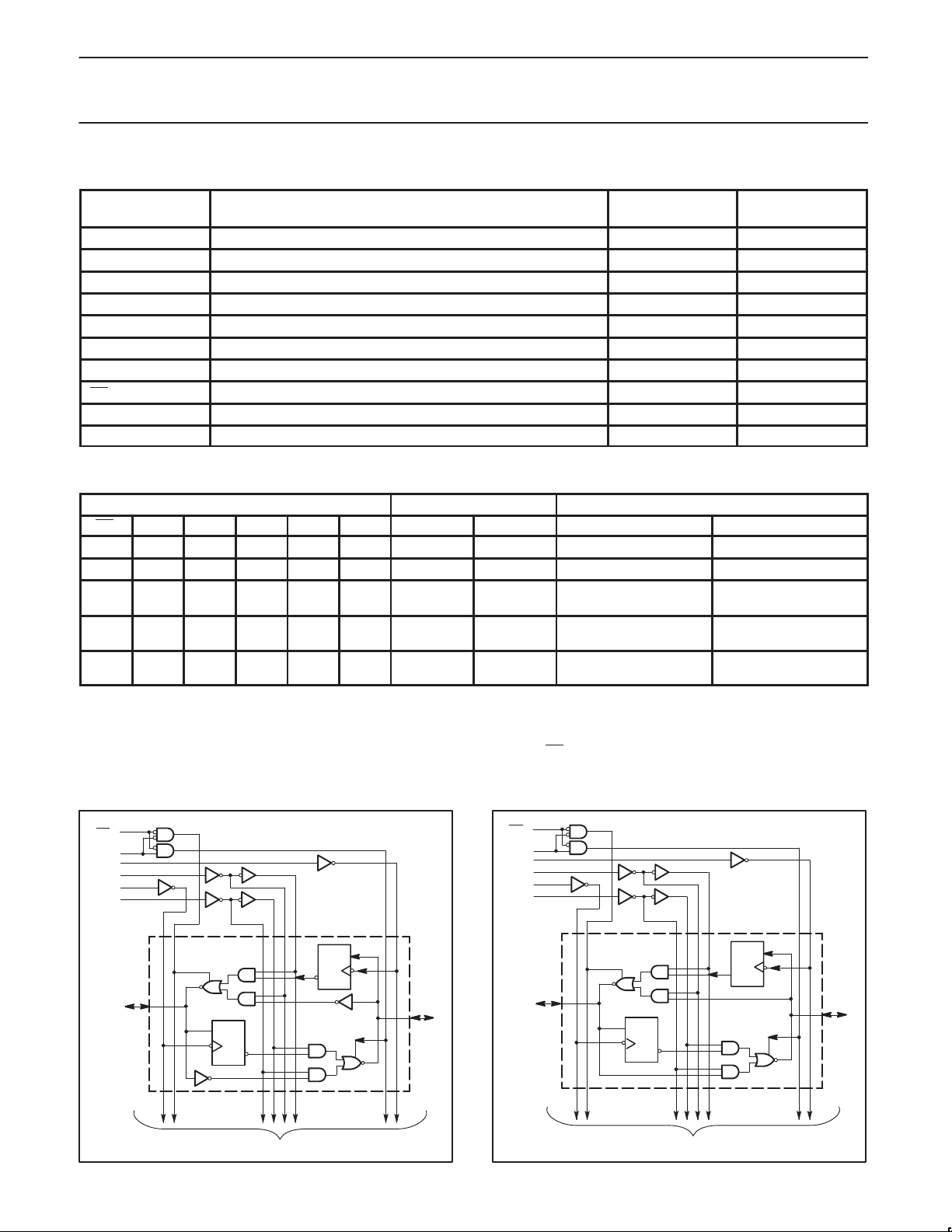
LOGIC DIAGRAM – 74F647
21
OE
3
DIR
23
CPBA
22
SBA
1
CPAB
2
SAB
1 of 8 Channels
4
A0
1D
C1
To 7 other channels
1992 Feb 28
LOGIC DIAGRAM – 74F649
21
OE
3
DIR
23
CPBA
22
SBA
1
CPAB
2
SAB
1D
C1
20
SF01202
B0
A0
1 of 8 Channels
4
1D
C1
To 7 other channels
4
1D
C1
20
B0
SF01203
 Loading...