

Philips 74f620, 74f 623 DATASHEETS

INTEGRATED CIRCUITS
74F620
Octal bus transceiver, inverting (3tate)
74F623
Octal bus transceiver, non–inverting
(3tate)
Product specification
IC15 Data Handbook
1989 Apr 06
Philips Semiconductors Product specification
74F620/74F623T ransceivers
74F620 Octal Bus Transceiver, Inverting (3-State)
74F623 Octal Bus Transceiver, Non-Inverting (3-State)
FEA TURES
•High-impedance NPN base inputs for reduced loading
(70µA in High and Low states)
•Ideal for applications which require high output drive and minimal
bus loading
•Octal bidirectional bus interface
•3-State buffer outputs sink 64mA and source 15mA
•74F620, inverting
•74F623, non-inverting
DESCRIPTION
The 74F620 is an octal transceiver featuring inverting 3-State
bus-compatible outputs in both send and receive directions. The
outputs are capable of sinking 64mA and sourcing up to 15mA,
providing very good capacitive drive characteristics. The 74F623 is
a non-inverting version of the 74F620.
These octal bus transceivers are designed for asynchronous
two-way communication between data buses. The control function
implementation allows for maximum flexibility in timing.
These devices allow data transmission from the A bus to the B bus
Enable inputs (OEBA
disable the device so that the buses are effectively isolated.
The dual-enable configuration gives the 74F620 and 74F623 the
capability to store data by the simultaneous enabling of OEBA
OEAB. Each output reinforces its input in this transceiver
configuration. Thus, when both control inputs are enabled and all
other data sources to the two sets of the bus lines are at high
impedance, both sets of bus lines (16 in all) will remain in their last
states.
TYPE
74F620 3.5ns 80mA
74F623 4.5ns 105mA
ORDERING INFORMATION
DESCRIPTION
20-pin plastic DIP N74F620N, N74623N SOT146-1
20-pin plastic SOL N74F620D, N74623D SOT163-1
and OEAB). The Enable inputs can be used to
TYPICAL
PROPAGATION
DELA Y
TYPICAL SUPPL Y CURRENT
(TOTAL)
COMMERCIAL RANGE
VCC = 5V ±10%,
T
= 0°C to +70°C
amb
PKG DWG #
or from the B bus to the A bus depending upon the logic levels at the
INPUT AND OUTPUT LOADING AND FAN-OUT TABLE
PINS DESCRIPTION
74F(U.L.)
HIGH/LOW
A0 - A7, B0 - B7 Data inputs 3.5/1.16 70µA/70µA
OEBA, OEAB Output Enable inputs 1.0/0.033 20µA/20µA
A0 - A7 Data outputs 150/40 3mA/24mA
B0 - B7 Data outputs 750/106.7 15mA/64mA
NOTE: One (1.0) FAST unit load is defined as: 20µA in the High state and 0.6mA in the Low state.
LOAD VALUE
HIGH/LOW
and
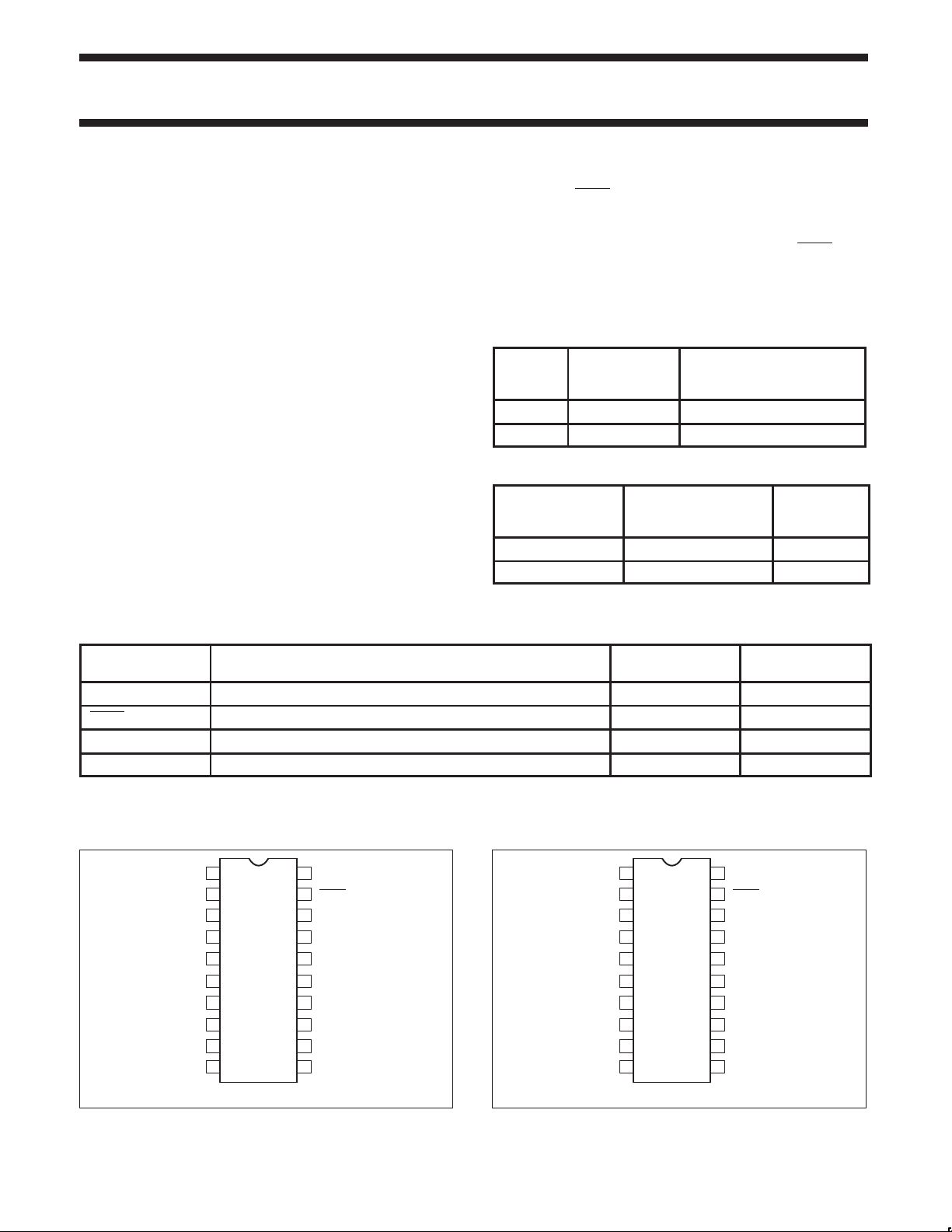
PIN CONFIGURATION – 74F620
1
OEAB
2
A0
3
A1
4
A2
5
A3
6
A4
7
A5
8
A6
9
A7
10 11
GND
1990 Apr 6 853–0379 96249
20
19
18
17
16
15
14
13
12
SF01124
V
CC
OEBA
B0
B1
B2
B3
B4
B5
B6
B7
PIN CONFIGURATION – 74F623
1
OEAB
2
A0
3
A1
4
A2
5
A3
6
A4
7
A5
8
A6
9
A7
10 11
GND
2
20
19
18
17
16
15
14
13
12
SF01124
V
CC
OEBA
B0
B1
B2
B3
B4
B5
B6
B7
Philips Semiconductors Product specification
74F620/74F623Transceivers
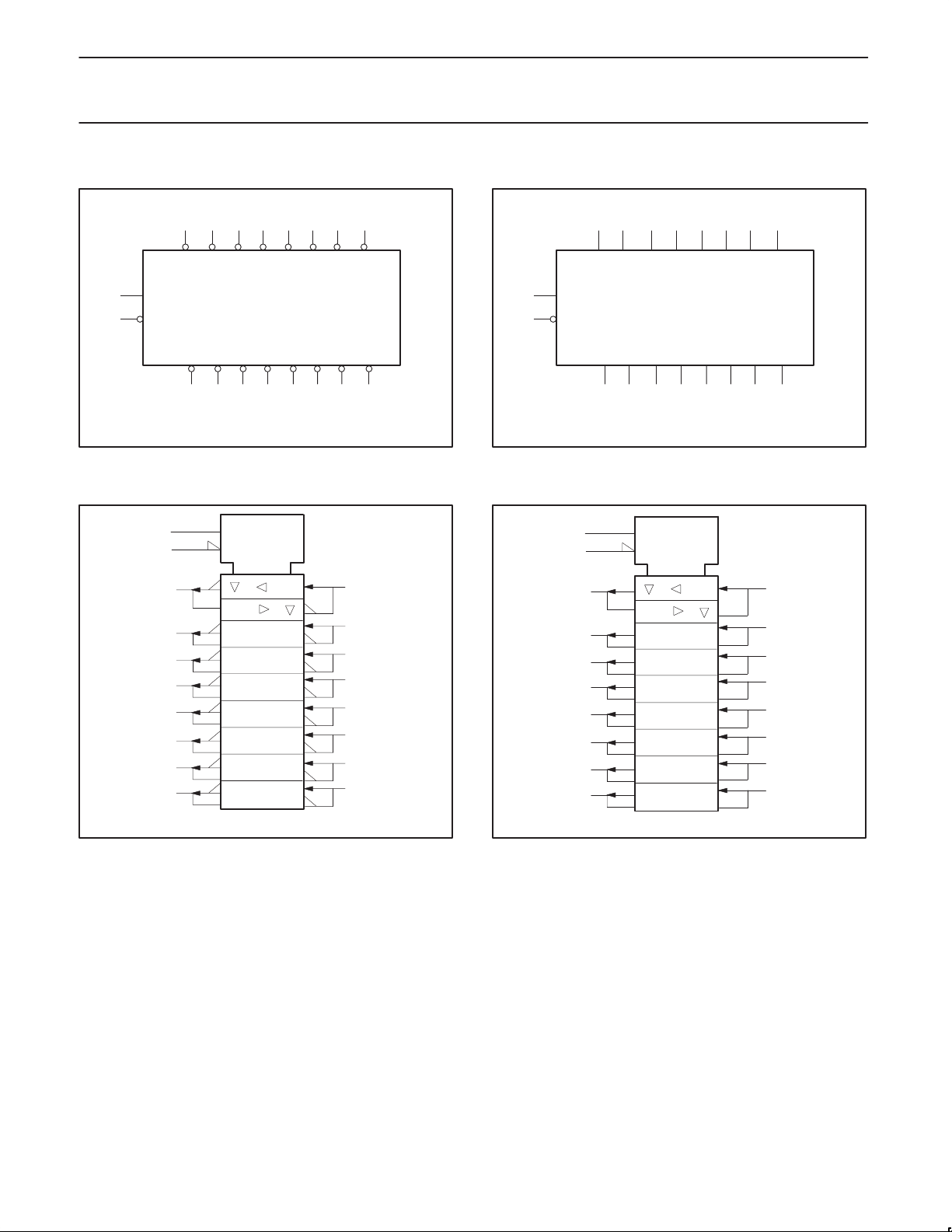
LOGIC SYMBOL – 74F620
89
SF01125
1
19
VCC= Pin 20
GND = Pin 10
23
A0 A1
OEAB
OEBA
B0 B1 B2 B3
18 17 16 15
456
A2 A3
A4 A5 A67A7
B4 B5 B611B7
14 13 12
IEC/IEEE SYMBOL (IEEE/IEC) – 74F620
1
19
EN1
EN2
2
3
4
5
6
7
8
9
1
2
18
17
16
15
14
13
12
11
LOGIC SYMBOL – 74F623
89
SF01126
1
19
VCC= Pin 20
GND = Pin 10
23
A0 A1
OEAB
OEBA
B0 B1 B2 B3
18 17 16 15 14 13 12 11
456
A2 A3
A4 A5 A67A7
B4 B5 B6 B7
IEC/IEEE SYMBOL (IEEE/IEC) – 74F623
1
19
EN1
EN2
2
3
4
5
6
7
8
9
1
2
18
17
16
15
14
13
12
11
1990 Apr 6
SF01127
SF01128
3
Philips Semiconductors Product specification
L
H
74F620/74F623Transceivers
LOGIC DIAGRAM – 74F620
19
OEBA
1
OEAB
2
A0
3
A1
4
A2
5
A3
6
A4
7
A5
8
A6
9
A7
LOGIC DIAGRAM – 74F623
19
OEBA
1
OEAB
18
B0
17
B1
16
B2
15
B3
14
B4
13
B5
12
B6
11
B7
2
A0
3
A1
4
A2
5
A3
6
A4
7
A5
8
A6
9
A7
18
B0
17
B1
16
B2
15
B3
14
B4
13
B5
12
B6
11
B7
VCC= Pin 20
GND = Pin 10
SF01129
FUNCTION TABLE
INPUTS OPERATING MODES
OEBA OEAB 74F620 74F623
L L B data to A bus B data to A bus
H H A data to B bus A data to B bus
H L Z Z
B data to A bus B data to A bus
A data to B bus A data to B bus
H = High voltage level
L = Low voltage level
X = Don’t care
Z = High impedance “off” state
VCC= Pin 20
GND = Pin 10
SF01130
1990 Apr 6
4
 Loading...