Philips 74f598 DATASHEETS

INTEGRATED CIRCUITS
74F598
8-bit shift register with input storage
registers (3-State)
Product specification
IC15 Data Handbook
1991 Oct 21

Philips Semiconductors Product specification
74F5988-bit shift register with input storage registers (3-State)
FEA TURES
• High impedance PNP base input for reduced loading (20µA in
High and Low states)
• 8–bit parallel storage register
The shift register load function has been modified to load when both
SHLD
and SHCP are Low. When SHCP is High the shift register
load operation is not performed. Data will be properly shifted on the
rising edge of SHCP when SHLD
is High.
• Shift register has asynchronous direct overriding reset
• Shift load SHLD is functional when SHCP is Low and locked out
when SHCP is High.
• Guaranteed shift frequency DC to 105MHz
• Parallel 3–State I/O storage register inputs and shift register
parallel outputs
DESCRIPTION
The 74F598 consists of an 8–bit storage register feeding a
parallel–in/serial–in, parallel–out/serial–out 8–bit shift register. Both
the storage register and shift register have positive edge–triggered
clocks. The shift register has asynchronous reset and when SHCP
is Low, it has asynchronous load.
TYPE
TYPICAL SHCP f
max
TYPICAL SUPPL Y
CURRENT (TOTAL)
74F598 100MHz 75mA
ORDERING INFORMATION
ORDER CODE
DESCRIPTION COMMERCIAL RANGE
= 5V ±10%,
V
CC
T
= 0°C to +70°C
amb
20–pin plastic DIP N74F598N SOT146-1
20–pin plastic SOL N74F598D SOT163-1
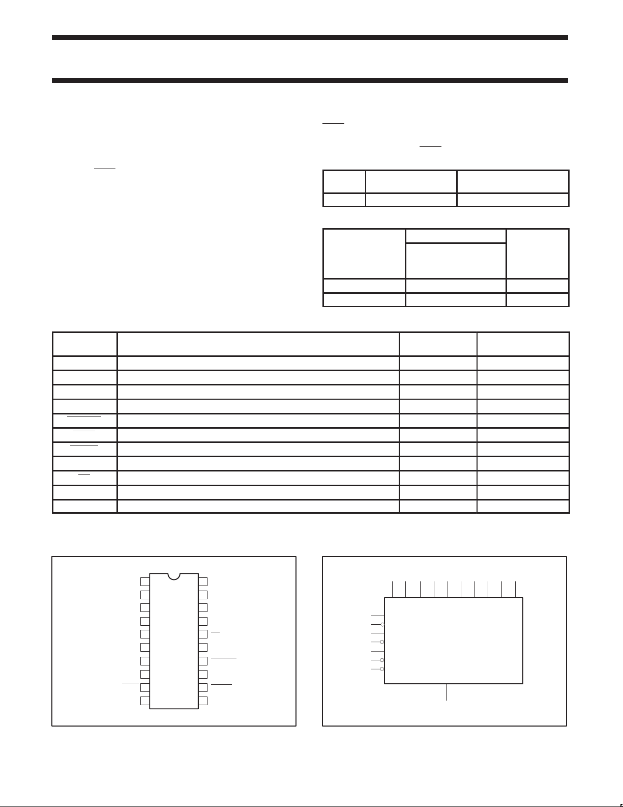
INPUT AND OUTPUT LOADING AND FAN OUT TABLE
PINS DESCRIPTION 74F (U.L.) High/
Low
I/On Parallel data input 1.0/0.033 20µA/20µA
Ds0, Ds1 Serial data inputs 1.0/0.033 20µA/20µA
SHCP Shift register clock pulse input 1.0/0.033 20µA/20µA
STCP Storage register clock pulse input 1.0/0.033 20µA/20µA
SHCPEN Shift register clock pulse enable input 1.0/0.033 20µA/20µA
SHLD Shift register load input (active Low) 1.0/0.033 20µA/20µA
SHRST Shift register reset input (active Low) 1.0/0.033 20µA/20µA
S Serial data select input 1.0/0.033 20µA/20µA
OE Output enable input 1.0/0.033 20µA/20µA
Qs Serial data output 50/33 1.0mA/20mA
I/On Parallel data outputs 150/40 3.0mA/24mA
Note to input and output loading and fan out table
1. One (1.0) FAST unit load is defined as: 20µA in the High state and 0.6mA in the Low state.
LOAD VALUE
High/Low
PKG DWG #
PIN CONFIGURATION
I/O0
1
I/O1
2
I/O2
3
I/O3
4
I/O4
5
I/O5
6
I/O6
7
I/O7
8
SHLD
9
GND
10 11
1991 Oct 21 853–1583 04407
20
19
18
17
16
15
14
13
12
SF00375
V
CC
S
DS0
DS1
OE
STCP
SHCPEN
SHCP
SHRST
Qs
LOGIC SYMBOL
19
16
15
14
13
12
= Pin 20
V
CC
GND = Pin 10
2
Ds018Ds117I/O01I/O12I/O23I/O34I/O45I/O56I/O67I/O7
S
OE
STCP
SHCPEN
SHCP
SHRST
SHLD
9
Qs
11
8
SF00376

Philips Semiconductors Product specification
74F5988-bit shift register with input storage registers (3-State)
IEC/IEEE SYMBOL
16
12
14
13
9
15
19
18
17
1
2
3
4
5
6
7
8
EN14
R
G4
4C5/4→
C2
C1
G1
, 5D
1
1, 5D
2D
6, 14
2D
7, 14
2D
13, 14
SRG8
Z6
3D
3D
Z7
3D
Z13
11
SF00377
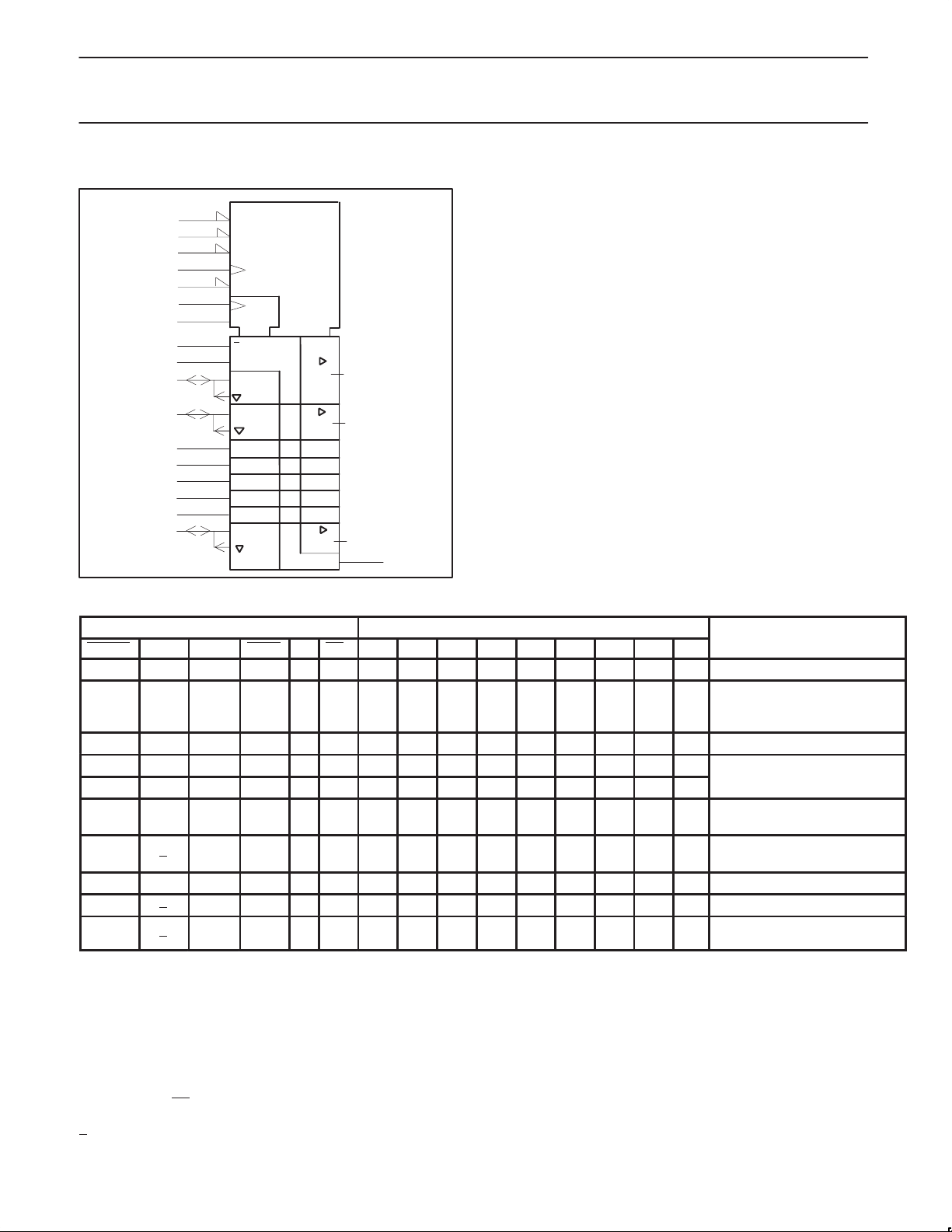
FUNCTION TABLE
INPUTS INPUTS/OUTPUTS OPERATING MODE
SHRST STCP SHCP SHLD S OE* I/O0 I/O1 I/O2 I/O3 I/O4 I/O5 I/O6 I/O7 Q7
L X L H X L L L L L L L L L L Clear shift register
Invalid, state of shift register in-
L X L L X L
X ↑ X X X H I0 I1 I2 I3 I4 I5 I6 I7 O7 Load data to storage register
H X ↑ H L L Ds0 O0 O1 O2 O3 O4 O5 O6 O6 Shift right
H X ↑ H H L Ds1 O0 O1 O2 O3 O4 O5 O6 O6
H ↑ L L X H I0 I1 I2 I3 I4 I5 I6 I7 O7
H ↑ L L X X O0 O1 O2 O3 O4 O5 O6 O7 O7
X X X X X H Z Z Z Z Z Z Z Z NC 3–State
H ↑ X H X X NC NC NC NC NC NC NC NC NC Hold
H ↑ H X X X NC NC NC NC NC NC NC NC NC
Notes to function table
D0 – D7 = The level of the steady state inputs to the serial multiplexer.
H = High voltage level
I0 – I7 = The level of the steady state input at the respective I/O terminal is loaded into the flip–flop while the flip–flop outputs ( except Q7) are isolated
from the I/O terminal.
L = Low voltage level
NC= No change
O0 – O7 = The level of the respective Qn flip–flop prior to the last clock Low–to–High transition
X = Don’t care
Z = High impedance ”off” state
* = When the OE
input is High, all I/O terminals are at the High impedance state, sequential operation or cleaning of the register is not affected.
↑ = Low–to–High clock transition
↑
= Not Low–to–High clock transition
determinate when signal is removed
Load data directly to shift register
Data transferred from storage
register to shift register
Hold (no storage or shift register
load
1991 Oct 21
3

Philips Semiconductors Product specification
74F5988-bit shift register with input storage registers (3-State)
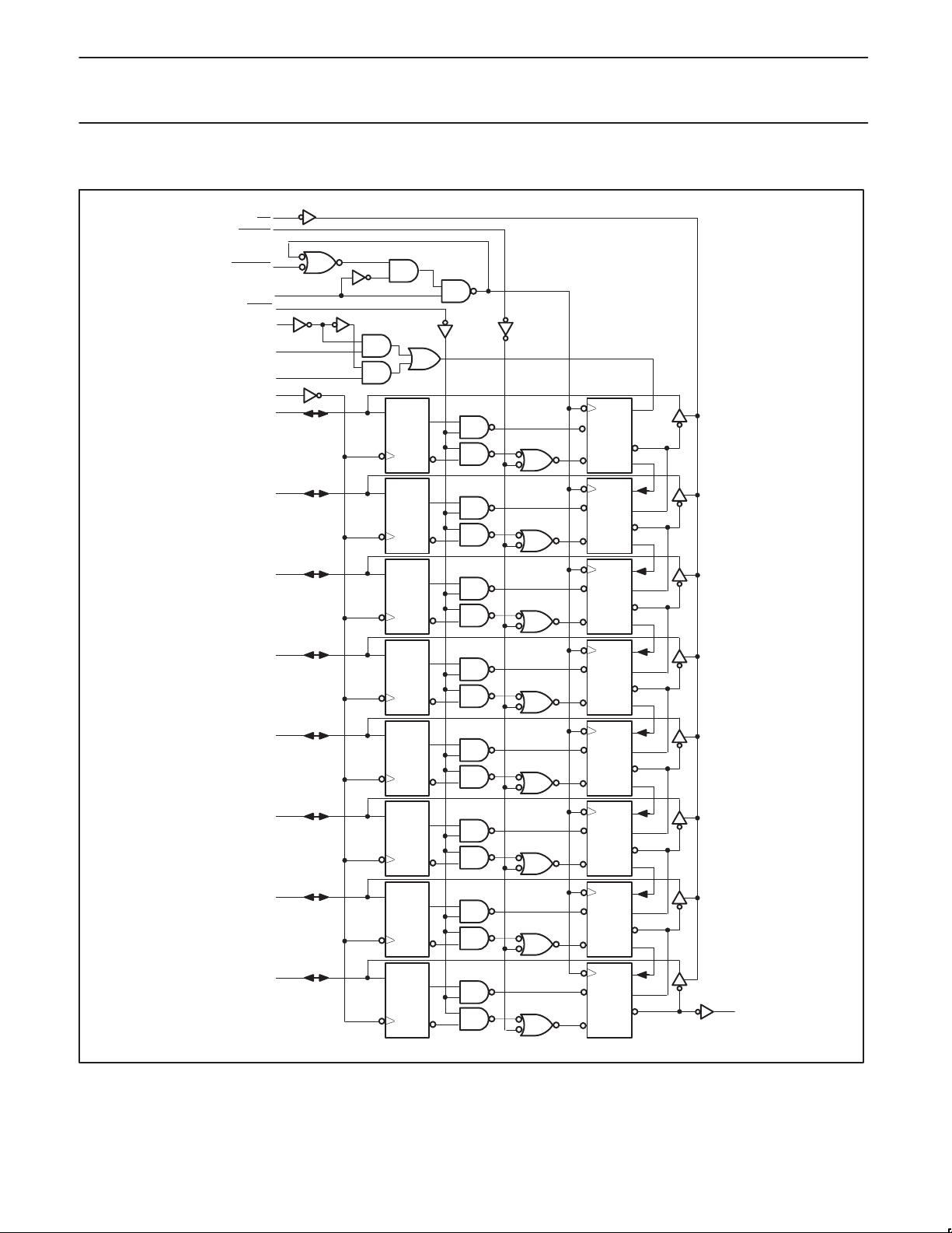
LOGIC DIAGRAM
16
OE
12
SHRST
14
SHCPEN
13
SHCP
9
SHLD
19
S
18
Ds0
17
Ds1
15
STCP
I/O0
I/O1
1
2
1D
C1
1D
2D
C2
S
R
C2
3S
S
3R
VCC = Pin 20
GND = Pin 10
I/O2
I/O3
I/O4
I/O5
I/O6
I/O7
C1
3
4
5
6
7
8
1D
C1
1D
C1
1D
C1
1D
C1
1D
C1
1D
C1
R
C2
3S
S
3R
R
C2
3S
S
3R
R
C2
3S
S
3R
R
C2
3S
S
3R
R
C2
3S
3R
S
R
C2
3S
S
3R
R
9
SF00378
Qs
1991 Oct 21
4

Philips Semiconductors Product specification
74F5988-bit shift register with input storage registers (3-State)
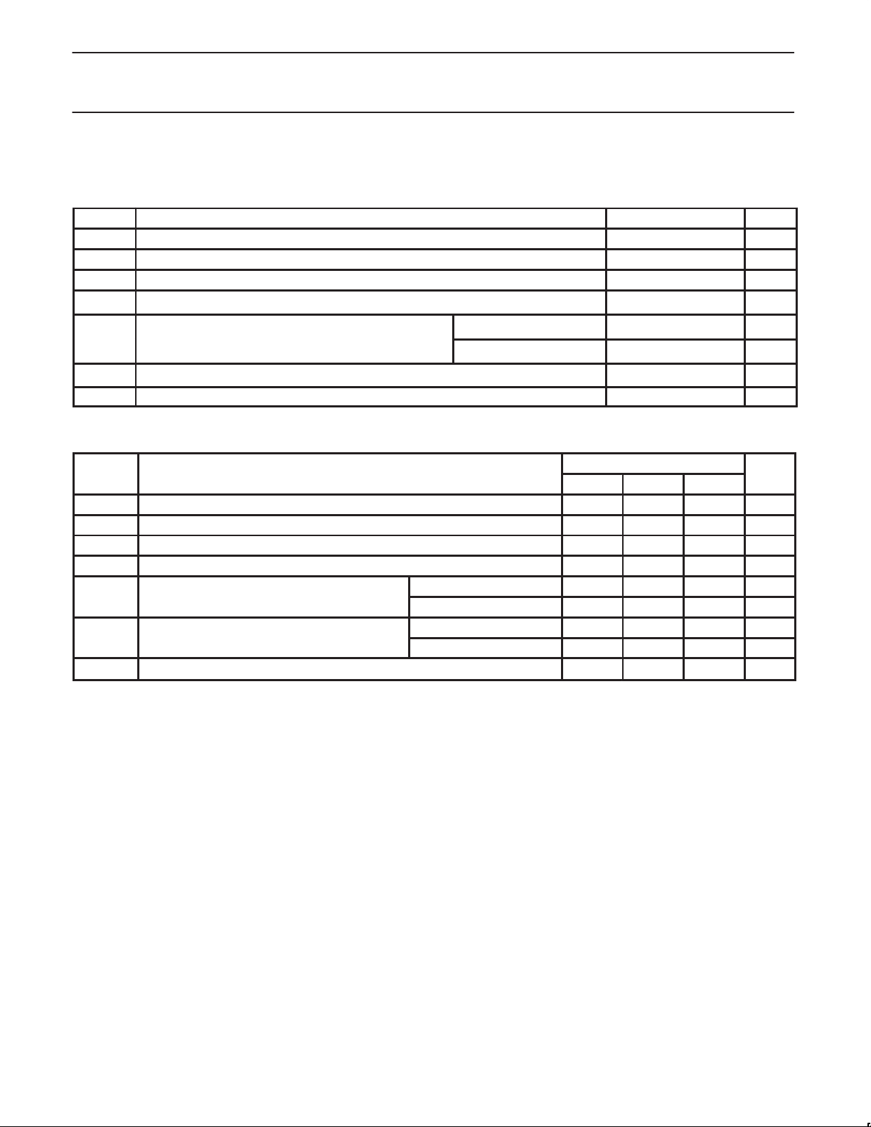
ABSOLUTE MAXIMUM RATINGS
(Operation beyond the limit set forth in this table may impair the useful life of the device. Unless otherwise noted these limits are over the
operating free air temperature range.)
SYMBOL
V
V
I
T
V
I
OUT
OUT
amb
T
Supply voltage –0.5 to +7.0 V
CC
Input voltage –0.5 to +7.0 V
IN
Input current –30 to +5 mA
IN
Voltage applied to output in High output state –0.5 to V
Current applied to output in Low output state Qs
Operating free air temperature range 0 to +70
Storage temperature range –65 to +150
stg
RECOMMENDED OPERATING CONDITIONS
SYMBOL PARAMETER LIMITS UNIT
T
V
V
V
I
I
OH
OL
amb
Supply voltage 4.5 5.0 5.5 V
CC
High–level input voltage 2.0 V
IH
Low–level input voltage 0.8 V
IL
I
Input clamp current –18 mA
Ik
High–level output current Qs –1 mA
Low–level output current Qs 20 mA
Operating free air temperature range 0 +70
PARAMETER RATING UNIT
CC
I/O0 – I/O7
40 mA
48 mA
V
°C
°C
MIN NOM MAX
I/O0 – I/O7 –3 mA
I/O0 – I/O7 24 mA
°C
1991 Oct 21
5
 Loading...