

Philips 74f540, 74f541 DATASHEETS

INTEGRATED CIRCUITS
74F540
Octal inverter buffer (3- State)
74F541
Octal buffer (3- State)
Product specification
IC15 Data Handbook
1990 Jan 08
Philips Semiconductors Product specification
74F540, 74F541Buffers
74F540 Octal Inverter Buffer (3-State)
74F541 Octal Buffer (3-State)
FEA TURES
•High impedance NPN base inputs for reduced loading
(20µA in High and Low states)
•Low power, light bus loading
•Functionally similar to the 74F240 and 74F241
TYPE
TYPICAL
PROPAGATION DELAY
74F540 3.5ns 58mA
74F541 5.5ns 55mA
TYPICAL SUPPL Y
CURRENT
(TOTAL)
•Provides ideal interface and increases fan-out of MOS
microprocessors
•Efficient pinout to facilitate PC board layout
•Octal bus interface
•3-State buffer outputs sink 64mA
•15mA source current
DESCRIPTION
The 74F540 and 74F541 are octal buffers that are ideal for driving
bus lines or buffer memory address registers. The outputs are
capable of sinking 64mA and sourcing up to 15mA, producing very
good capacitive drive characteristics. The devices feature input and
outputs on opposite sides of the package to facilitate printed circuit
board layout.
INPUT AND OUTPUT LOADING AND FAN-OUT TABLE
PINS DESCRIPTION
I0–I7 Data inputs 1.0/0.033 20µA/20µA
OE0, OE1 3-State output enable inputs (active Low) 1.0/0.033 20µA/20µA
Y0 - Y7 Data outputs (74F541) 750/106.7 15mA/64mA
Y0 - Y7 Data outputs (74F540) 750/106.7 15mA/64mA
NOTE: One (1.0) FAST Unit Load is defined as: 20µA in the High state and 0.6mA in the Low state.
ORDERING INFORMATION
COMMERCIAL RANGE
DESCRIPTION
20-Pin Plastic DIP N74F540, N74F541N SOT146-1
20-Pin Plastic SOL N74F540D, N74F541D SOT163-1
VCC = 5V ±10%,
T
= 0°C to +70°C
amb
74F(U.L.)
HIGH/LOW
PKG DWG #
LOAD VALUE
HIGH/LOW
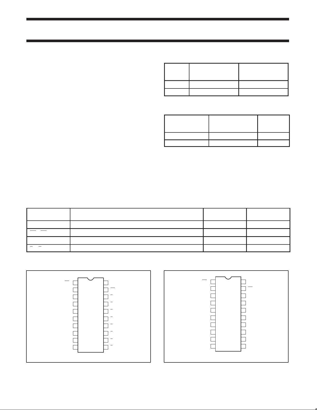
PIN CONFIGURATION – 74F540
OE
0
1
I0
2
I1
3
I2
4
I3
5
I4
6
I5
7
I6
8
I7
9
10 11
GND
1990 Jan 08 853–0068 98494
20
19
18
17
16
15
14
13
12
SF01060
V
OE1
Y
Y
Y
Y3
Y4
Y
Y6
Y
CC
0
1
2
5
7
PIN CONFIGURATION – 74F541
OE
0
1
I0
2
I1
3
I2
4
I3
5
I4
6
I5
7
I6
8
I7
9
10 11
GND
2
20
19
18
17
16
15
14
13
12
SF01021
V
OE1
Y0
Y1
Y2
Y3
Y4
Y5
Y6
Y7
CC
Philips Semiconductors Product specification
74F540, 74F541Buffers
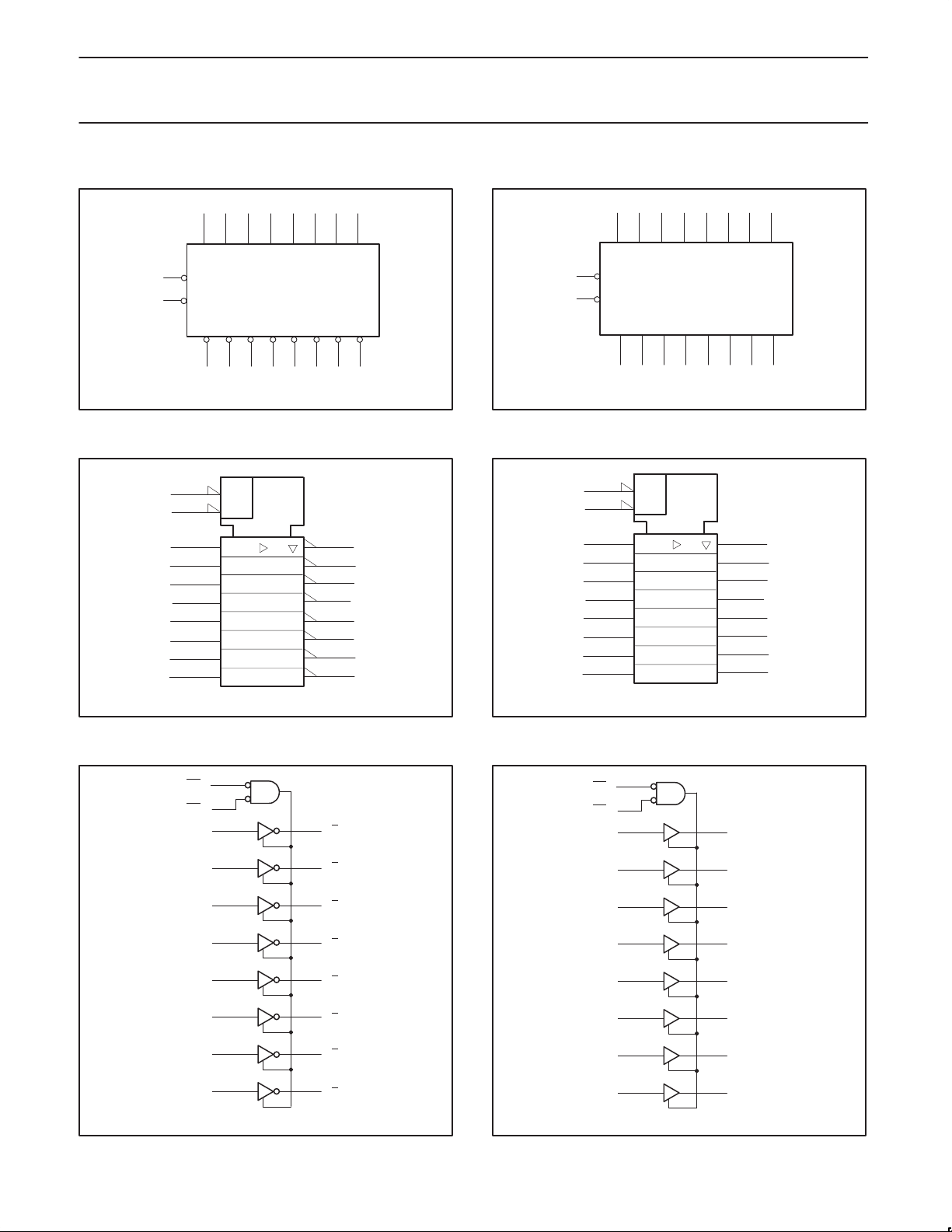
LOGIC SYMBOL – 74F540
= Pin 20
V
CC
GND = Pin 10
234
I0 I1 I4 I5 I6 I7
1
OE0
19
OE1
Y0 Y1 Y4 Y5 Y6 Y7
18 17 16 15 14 13 12 11
56789
I3I2
Y2 Y3
LOGIC SYMBOL (IEEE/IEC) – 74F540
1
19
2
3
4
5
6
7
8
9
&
EN
SF01022
18
17
16
15
14
13
12
11
LOGIC SYMBOL – 74F541
= Pin 20
V
CC
GND = Pin 10
234
I0 I1 I4 I5 I6 I7
1
OE0
19
OE1
Y0 Y1 Y4 Y5 Y6 Y7
18 17 16 15 14 13 12 11
56789
I3I2
Y2 Y3
LOGIC SYMBOL (IEEE/IEC) – 74F541
1
19
2
3
4
5
6
7
8
9
&
EN
SF01023
18
17
16
15
14
13
12
11
LOGIC DIAGRAM – 74F540
1
OE0
19
OE
1
2
I0
3
I1
4
I2
5
I3
6
I4
7
I5
8
I6
9
VCC= Pin 20
GND = Pin 10
I7
SF01024
18
17
16
15
14
13
12
11
SF01026
SF01025
LOGIC DIAGRAM – 74F541
1
OE0
19
1
OE
Y0
Y
1
2
Y
Y
3
4
Y
Y
5
6
Y
Y
7
VCC= Pin 20
GND = Pin 10
2
I0
3
I1
4
I2
5
I3
6
I4
7
I5
8
I6
9
I7
18
17
16
15
14
13
12
11
SF01027
Y0
Y1
Y2
Y3
Y4
Y5
Y6
Y7
1990 Jan 08
3
 Loading...