

Philips 74f3893 DATASHEETS

INTEGRATED CIRCUITS
74F3893
Quad futurebus backplane transceiver
Product specification
IC15 Data Handbook
1991 Jan 18
Philips Semiconductors Product specification
74F3893Quad Futurebus backplane transceiver
FEA TURES
• Quad backplane transceiver
• Drives heavily loaded backplanes with equivalent load
impedances down to 10 ohms
• Futurebus drivers sink 100mA
• Reduced voltage swing (1 volt) produces less noise and
reduces power consumption
• High speed operation enhances performance of backplane
buses and facilitates incident wave switching
• Compatible with IEEE 896 and IEEE 1194.1 Futurebus
Standards
• Built–in precision band–gap (BG) reference provides
accurate receiver thresholds and improved noise immunity
• Glitch–free power up/power down operation on all outputs
• Pin and function compatible with NSC DS3893
DESCRIPTION
The 74F3893 is a quad backplane transceivers and is
intended to be used in very high speed bus systems.
The 74F3893 interfaces to ‘Backplane Transceiver Logic’
(BTL). BTL features a reduced (1V to 2V) voltage swing for
lower power consumption and a series diode on the drivers
to reduce capacitive loading (< 5pF).
Incident wave switching is employed, therefore BTL
propagation delays are short. Although the voltage swing is
much less for BTL, so is its receiver threshold region,
therefore noise margins are excellent.
BTL offers low power consumption, low ground bounce, EMI
and crosstalk, low capacitive loading, superior noise margin
and low propagation delays. This results in a high
bandwidth, reliable backplane.
The 74F3893 has four TTL outputs (Rn) on the receiver
side with a common receiver enable input (RE
data inputs (Dn) which are also TTL. These data inputs are
NANDed with the data enable input (DE). The four I/O pins
(bus side) are futurebus compatible, sink a minimum of
100mA, and are designed to drive heavily loaded
backplanes with load impedances as low as 10 ohms. All
outputs are designed to be glitch–free during power up and
down.
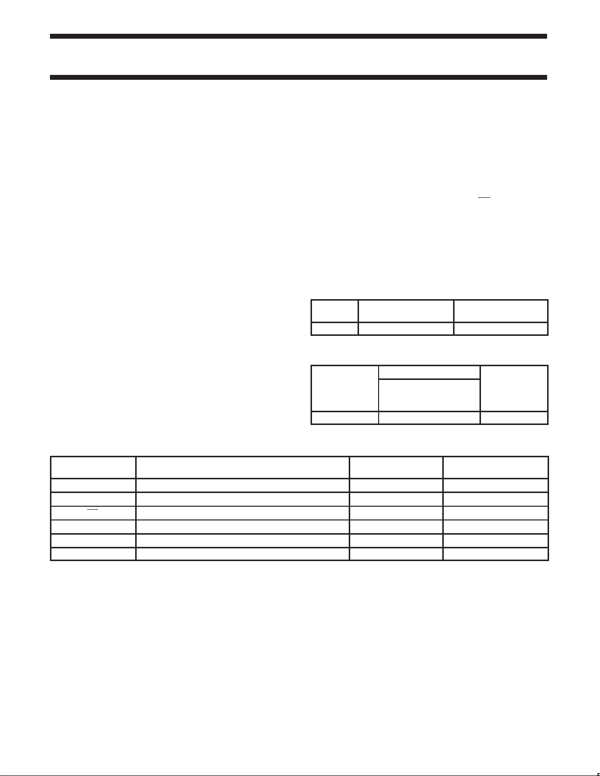
TYPE TYPICAL
74F3893 3.0ns 55mA
PROPAGATION DELAY
ORDERING INFORMATION
ORDER CODE
DESCRIPTION COMMERCIAL RANGE
= 5V ±10%,
V
CC
T
= 0°C to +70°C
amb
20-pin PLCC N74F3893A SOT380-1
). It has four
TYPICAL SUPPL Y
CURRENT( TOTAL)
PKG DWG #
INPUT AND OUTPUT LOADING AND FAN OUT TABLE
PINS DESCRIPTION
D0 – D3 Data inputs 1.0/0.067 20µA/40µA
DE Data enable input 1.0/0.33 20µA/200µA
RE Receiver enable input 1.0/0.067 20µA/40µA
I/O0 – I/O3 Bus inputs 5.0/0.033 100µA/20µA
I/O0 – I/O3 Bus outputs OC/166.7 OC/100mA
R0 – R7 Receiver outputs 150/40 3mA/24mA
Notes to input and output loading and fan out table
One (1.0) FAST unit load is defined as: 20µA in the high state and 0.6mA in the low state.
OC= Open collector.
74F (U.L.)
HIGH/LOW
LOAD VALUE
HIGH/LOW
January 18, 1991 853-1397 01496
2
Philips Semiconductors Product specification
74F3893Quad Futurebus backplane transceiver
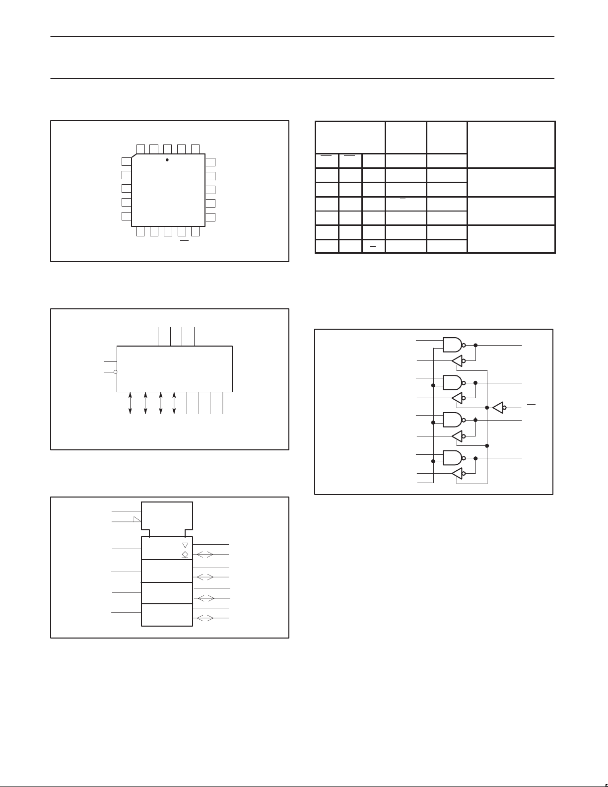
PIN CONFIGURATION
3212019
4
D1
5
R1
LOGIC GND
6
7
D2
8
R2
9
LOGIC SYMBOL
DE
11
RE
12
I/O0 I/O1 1/O2 I/O3 R0 R1 R2 R3
= Pin 1,
V
CC
LOGIC GND = Pin 8
BUS GND = Pin 13, 16, 19
BG GND = Pin 20
18 17 15 14 3 5 8 10
IEC/IEEE SYMBOL
V
GND
D0R0
CC
PLCC
DER3D3
2 4 7 9
D0 D1 D2 D3
BG
RE
BUS
GND
13121110
BUS
GND
18
I/O0
17
I/O1
BUS GND
16
15
I/O2
14
I/O3
SF00573
SF00574
FUNCTION TABLE
INPUT/
INPUTS
OUT-
PUT
DE RE Dn I/On Rn MODE
H L L H L Transmit to bus
H L H L H
H H Dn Dn Z Receiver 3–state,
L H X H Z transmit to bus
L L X H L Receive, I/On = inputs
L L X L H
Notes to function table
1. H = High voltage level
2. L = Low voltage level
3. X = Don’t care
4. Z = High impedance ”off” state
OUT-
PUT
OPERATING
LOGIC DIAGRAM
VCC = Pin 1
LOGIC GND = Pin 6
BUS GND = Pin 13, 16, 19
BG GND = Pin 20
D0
D2
D3
DE
2
3
R0
4
D1
5
R1
7
8
R2
9
10
R3
11
18
17
12
15
14
SF00576
I/O0
I/O1
RE
I/O2
I/O3
January 18, 1991
11
12
2
4
7
9
EN1
EN2
1D
2
3
18
5
17
7
15
9
14
SF00575
3
 Loading...