

Philips 74f385 DATASHEETS
Philips Semiconductors Product specification
74F385Quad serial adder/subtractor
1
1989 Sep 20 853–0868 97678
FEATURES
•Four independent adders/subtractors
•Two’s complement arithmetic
•Synchronous operation
•Common Clear and Clock
•74F385 is designed for use with serial multipliers in implementing
digital filters and butterfly networks in fast Fourier transforms
DESCRIPTION
The 74F385 contains four independent adder/subtractor elements
with common Clock and Master Reset. Each adder/subtractor
contains a sum flop-flop and a carry flip-flop for synchronous
operations. Flip-flop state changes occur on the rising edge of the
Clock Pulse (CP) input signal. The Select (S) input should be Low
for the Add (A plus B) mode and High for the Subtract (A minus B)
mode. A Low signal on the asynchronous Master Reset (MR
) input
clears the sum flip-flop and resets the Carry flip-flop to zero in the
Add mode or presets it to one in the Subtract mode.
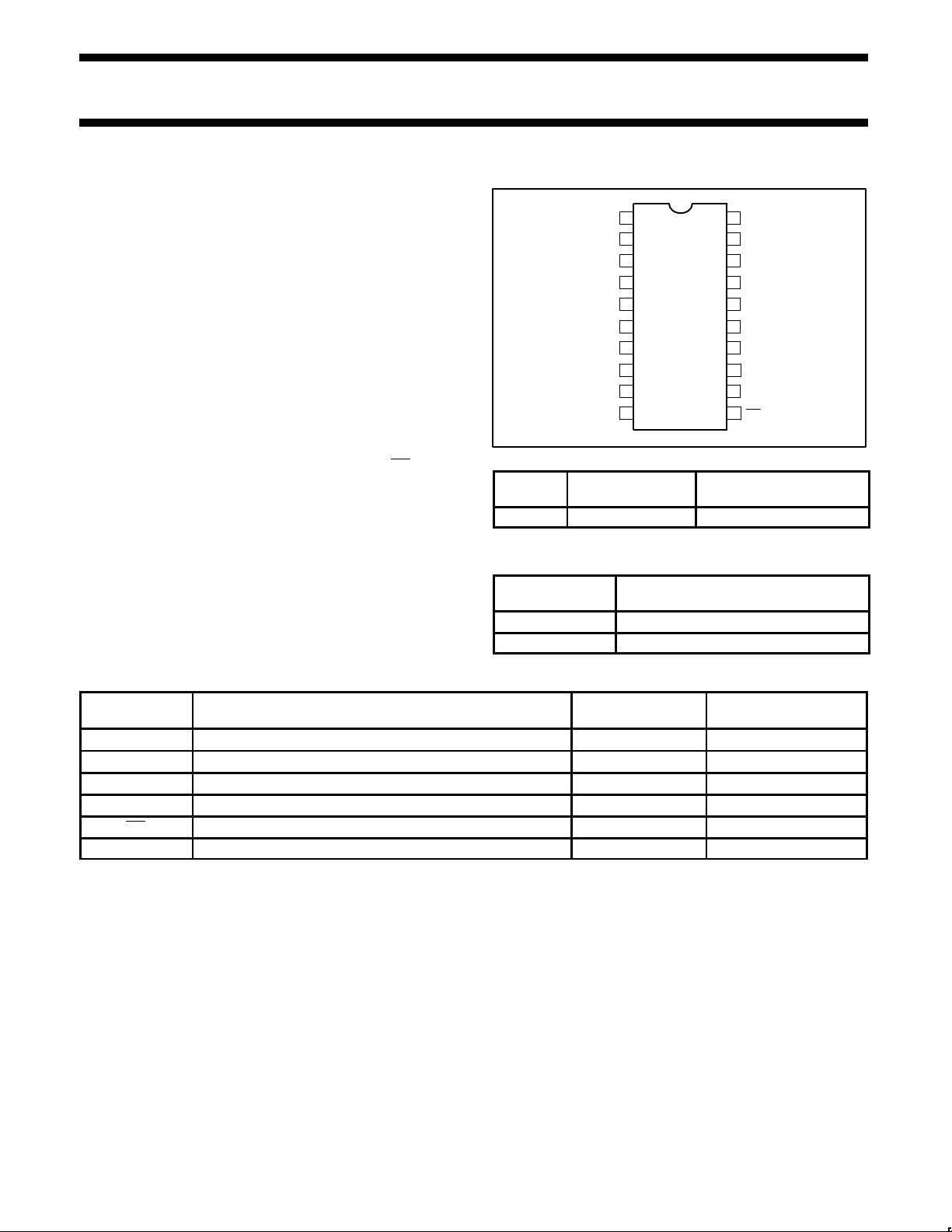
PIN CONFIGURATION
20
19
18
17
16
15
147
6
5
4
3
2
1
138
V
CC
CP
F0
S0
B0
A0
A1
B1
S1
F1
GND
F3
S3
B3
A3
A2
B2
S2
F2
MR
SF00928
129
1110
TYPICAL f
MAX
TYPICAL SUPPL Y
CURRENT (TOTAL)
74F385 140 MHz 55mA
ORDERING INFORMATION
DESCRIPTION
COMMERCIAL RANGE
VCC = 5V ±10%, T
amb
= 0°C to +70°C
20-pin plastic DIP N74F385N
20-pin plastic SO N74F385D
INPUT AND OUTPUT LOADING AND FAN OUT TABLE
PINS DESCRIPTION 74F (U.L.)
HIGH/LOW
LOAD VALUE
HIGH/LOW
A0 – A3 A operand inputs 1.0/1.0 20µA/0.6mA
B0 – B3 B operand inputs 1.0/1.0 20µA/0.6mA
S0 – S3 Function select inputs 1.0/1.0 20µA/0.6mA
CP Clock pulse input (active rising edge) 1.0/1.0 20µA/0.6mA
MR Asynchronous Master Reset input (active Low) 1.0/1.0 20µA/0.6mA
F0–F3 Sum or difference outputs 50/33 1.0mA/20mA
NOTE:
One (1.0) FAST unit load is defined as: 20µA in the High state and 0.6mA in the Low state.
TYPE
Philips Semiconductors Product specification
74F385Quad serial adder/subtractor
1989 Sep 20
2
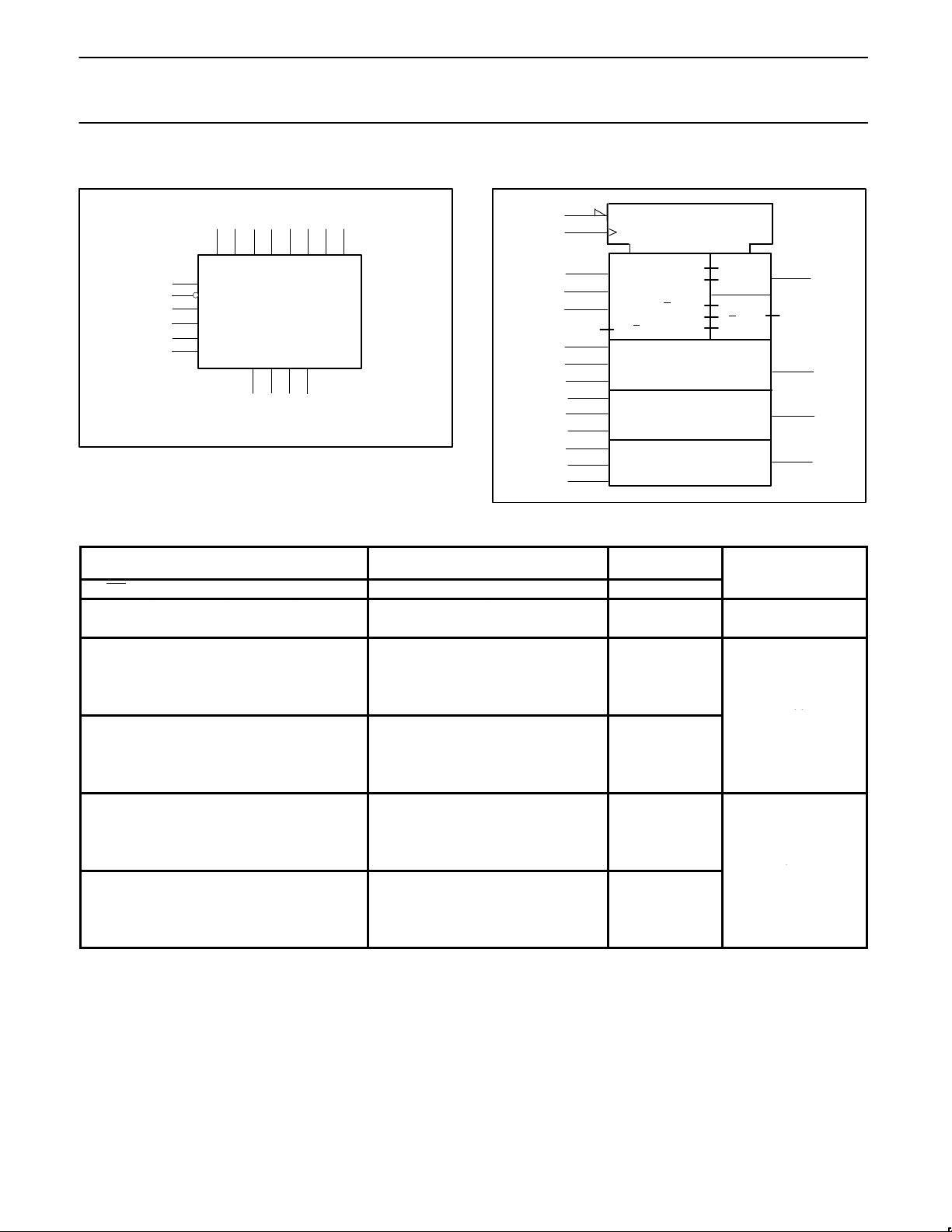
LOGIC SYMBOL
F0 F1 F2 F3
V
CC
= Pin 20
GND = Pin 10
A0 B0 A1 B1 A2 B2 A3 B3
5 4 6 7 15 14 16 17
CP
MR
S0
S1
S2
S3
1
11
3
8
13
18
2 9 12 19
SF00929
IEC/IEEE SYMBOL
9
11
19
5
P
SF00930
8
6
7
13
15
14
18
16
Q
11
1
2
17
M3
4(3CI/ 3BI)
3C
O/ 3BO
/P–Q
Z4
2D
R
2D
3R
3S
3
4
Z1
C2
FUNCTION TABLE
INPUTS
CARRY
FLIP-FLOP STATE
OUTPUTS
OPERATING
MR S A B Before↑ After↑ F
MODE
L L X X L L L
L H X X H H L
Clear
H L L L L L L
H L L L H L H
H L L H L L H
H L L H H H L
H L H L L L H
Add
H L H L H H L
H L H H L H L
H L H H H H H
H H L L L L H
H H L L H H L
H H L H L L L
H H L H H L H
H H H L L H L
Subtract
H H H L H H H
H H H H L L H
H H H H H H L
H = High voltage level
L = Low voltage level
X = Don’t care
↑ = Low-to-High Clock transition
 Loading...