

Philips 74f382 DATASHEETS

INTEGRATED CIRCUITS
74F382
Arithmetic Logic Unit
Product specification
IC15 Data Handbook
1990 Jul 12
Philips Semiconductors Product specification
74F382Arithmetic logic unit
FEA TURES
•Performs six arithmetic and logic functions
•Selectable Low (clear) and High (preset) functions
•Low-input loading minimizes drive requirements
•Carry output for ripple expansion
•Overflow output for Two’s Complement arithmetic
DESCRIPTION
The 74F382 performs three arithmetic and three logic operations on
two 4-bit words, A and B. Two additional Select (S0–S2) input codes
force the Function outputs Low or High. An overflow output is
provided for convenience in Two’s Complement arithmetic.
A carry output is provided for ripple expansion. For high-speed
expansion using a carry look-ahead generator, refer to the 74F381
data sheet.
Signals applied to the Select inputs, S0–S2, determine the mode of
operation, as indicated in the Function Select Table. An extensive
listing of input and output levels is shown in the Function Table. The
circuit performs the arithmetic functions for either active-HIgh or
active-Low operands, with output levels in the same convention. In
the subtract operating modes, it is necessary to force a carry (High
for active-HIgh operands, Low for active-Low operands) into the Cn
input of the least significant package. Ripple expansion is illustrated
in Figure 1. The overflow output OVR is the Exclusive-OR of Cn+3
and Cn+4; a High signal on OVR indicates overflow in Two’s
complement operation (See Table 2 for Two’s complement
arithmetic). Typical delays for Figure 1 are given in Table 1. When
the 74F382 is cascaded to handle word lengths longer than 4 bits,
only the most significant overflow (OVR) output is used.
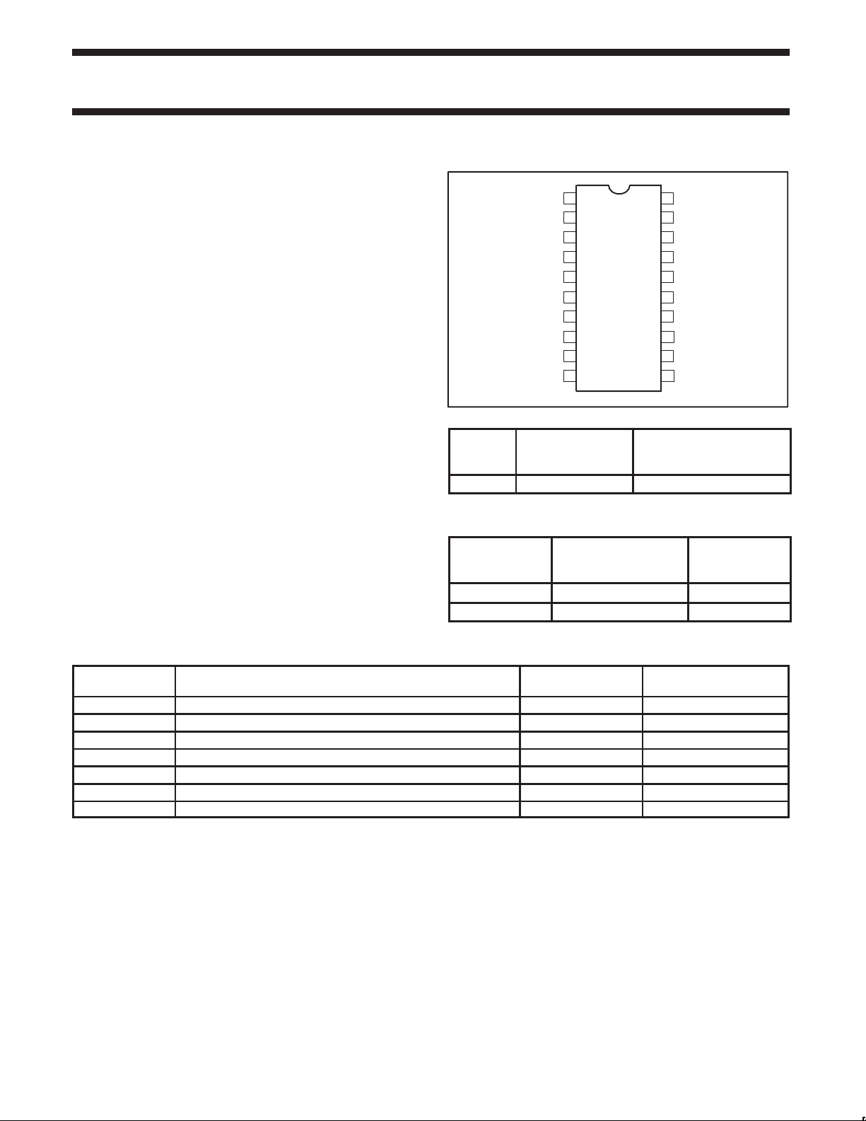
PIN CONFIGURATION
1
A1
2
B1
3
A0
4
B0
5
S0
6
S1
S2
F0
F1
GND
TYPICAL
TYPE
PROPAGATION
DELAY
74F382 7.0ns 54mA
20
V
CC
19
A2
18
B2
17
A3
16
B3
15
Cn
147
Cn+4
138
OVR
129
F3
1110
F2
TYPICAL SUPPL Y
CURRENT (TOTAL)
ORDERING INFORMATION
COMMERCIAL RANGE
V
DESCRIPTION
20-pin plastic DIP N74F382N SOT146-1
20-pin plastic SO N74F382D SOT163-1
= 5V ±10%,
CC
T
= 0°C to +70°C
amb
PKG DWG #
SF00935
INPUT AND OUTPUT LOADING AND FAN OUT TABLE
PINS DESCRIPTION
A0 – A3 A operand inputs 1.0/4.0 20µA/2.4mA
B0 – B3 B operand inputs 1.0/4.0 20µA/2.4mA
S0 – S2 Function select inputs 1.0/1.0 20µA/0.6mA
Cn Carry input 1.0/5.0 20µA/3.0mA
Cn+4 Carry output 50/33 1.0mA/20mA
OVR Overflow output 50/33 1.0mA/20mA
F0–F3 Outputs 50/33 1.0mA/20mA
NOTE:
One (1.0) FAST unit load is defined as 20µA in the High state and 0.6mA in the Low state.
74F (U.L.)
HIGH/LOW
LOAD VALUE
HIGH/LOW
1990 Jul 12 853–0419 99966
2
Philips Semiconductors Product specification
74F382Arithmetic logic unit
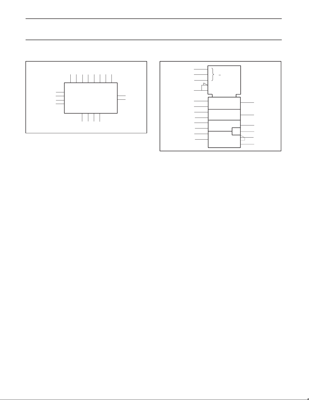
LOGIC SYMBOL
15
5
6
7
V
= Pin 20
CC
GND = Pin 10
3 4 1 2 19 18 17 16
A0 B0 A1 B1 A2 B2 A3 B3
Cn
S0
S1
S2
F0 F1 F2 F3
891112
OVR
Cn+4
13
14
SF00936
IEC/IEEE SYMBOL
5
6
7
15
3
4
1
2
19
18
17
16
0
2
(1/2) Bl
3 Cl
P
Q
P
Q
P
Q
P
Q
M
ALU
0
7
[1]
[2]
[4]
BO/CO
BO/CO
[8]
=1
(1/2)BO
3CO
8
9
11
13
14
12
SF00937
1990 Jul 12
3
Philips Semiconductors Product specification
74F382Arithmetic logic unit
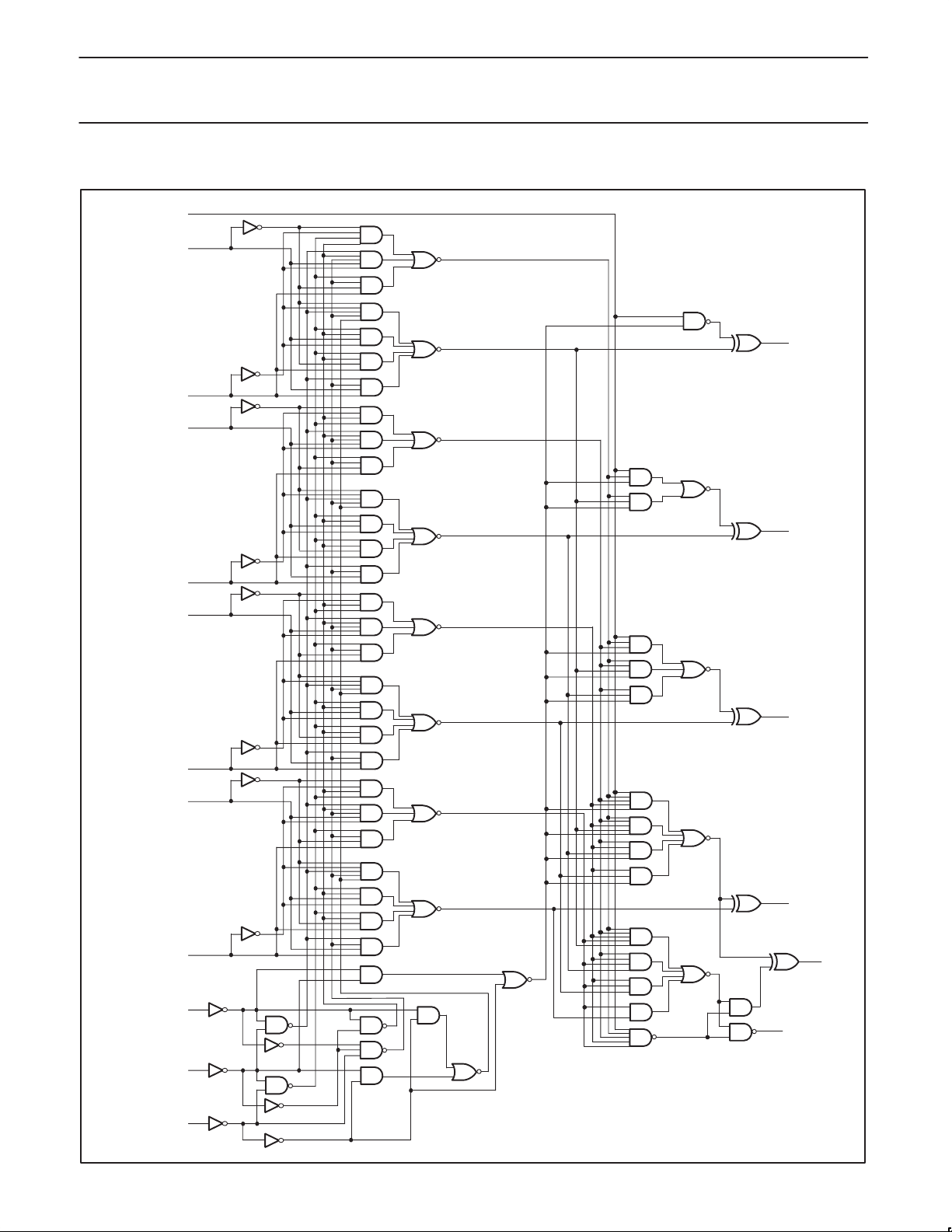
LOGIC DIAGRAM
15
Cn
3
A0
8
F0
4
B0
1
A1
9
F1
2
B1
19
A2
11
F2
18
B2
17
A3
12
F3
16
B3
13
OVR
VCC = Pin 20
GND = Pin 10
1990 Jul 12
5
S0
6
S1
7
S2
14
Cn+4
SF00938
4
 Loading...